4 марта южнокорейский техногигант Samsung Electronics получил правительственную награду «Крупнейший налогоплательщик» за уплату налогов в размере более 6 миллиардов долларов США в 2017 году благодаря процветающему бизнесу по производству микросхем. Samsung, ведущий мировой производитель чипов памяти, выплатил в казну Южной Кореи 6,8 триллиона вон (6,04 миллиарда долларов США) в виде подоходного налога с предприятий за 2017-й. Такими образом, Samsung остаётся крупнейшим налогоплательщиком в стране. Другой корейский чипмейкер, SK hynix, также получил награду, поскольку направил в госфонды 2,2 триллиона вон налоговых отчислений. Samsung и SK hynix объявили об огромной прибыли в 2017 году, так как устойчивый глобальный спрос на чипы укрепил их позиции. Министерство налогов и сборов Республики Корея сообщило, что Hana Bank стал корпоративным налогоплательщиком №3 с 600 миллиардами вон. Также награды получили 13 других компаний, которые выплатили налоги в размере не менее 100 миллиардов вон. Кроме того, министерство отметило 1089 «образцовых налогоплательщиков» в ходе официальной церемонии в Сеуле по случаю 53-го Дня налогоплательщика, сообщает бизнес-портал The Investor. Samsung wins ‘high taxpayer’ award Korean tech behemoth Samsung Electronics won a “large-sum taxpayer” award from the government on March 4 for paying more than US$6 billion in taxes in 2017 thanks to its booming chip business, the Finance Ministry said. Samsung, the world’s leading memory chipmaker, was honored for paying 6.8 trillion won (US$6.04 billion) in corporate income taxes for the fiscal year 2017. Samsung was the country’s top corporate taxpayer. Another Korean chip giant, SK hynix also received the award by paying 2.2 trillion won in taxes. Samsung and SK hynix posted stellar earnings in 2017 as the robust global chip market bolstered their bottom lines. The ministry said Hana Bank, which was the country’s No. 3 corporate taxpayer by paying 600 billion won, and 13 other companies also won the award that goes to companies paying taxes of 100 billion won or more. In addition, 1,089 “exemplary taxpayers” were honored during a ceremony in Seoul to mark the 53rd Taxpayer’s Day, the ministry added.
Всемирная организация интеллектуальной собственности (World Intellectual Property Organization, WIPO) опубликовала патентную документацию Samsung на новую систему питания для телевизоров следующего поколения. Транснациональный электронный гигант нашёл способ полностью избавить ТВ-панели от проводов. То есть это означает отказ от традиционного кабеля питания в пользу специальной системы беспроводной передачи энергии, а цифровой аудио/видеопоток предполагается транслировать с помощью технологии высокоскоростной беспроводной передачи, используя наработки в области 5G. Решение включает продолговатый приёмный модуль, монтирующийся в тыльной части телевизионной панели, подвешенной на стену. Передающий блок, в свою очередь, может быть установлен под дисплеем — например, на стойке для техники. Беспроводная передача энергии осуществляется посредством метода магнитной индукции. Такую технологию, как известно, используют устройства с поддержкой стандарта Qi. Заявка на патент была подана компанией Samsung в ещё марте прошлого года, но обнародован документ только сейчас. Разумеется, в патентных документах никогда не указывается информация о датах внедрения новой технологию в коммерческие продукты. Samsung patents wireless TV with no power cable Could Samsung be on the cusp of a fully wireless TV? A recent patent hints that a Samsung TV without any pesky cables could be around the corner. Spotted by LetsGoDigital, the patent was filed in March 2018 but only released publicly in late February of this year. The patent revolves around a wireless power transceiver, which would make the prospective television the first of its kind to transmit power across the room rather than relying on a power cable - increasingly seen as an eyesore next to Samsung's premium design sets. The transceiver takes the form of a magnetic bar attached to the rear of the television, given that panels themselves are too thin to house anything of this kind. It would then require a separate power transmitter (plugged into the mains) to keep the TV running. We're not surprised to see Samsung investigating wireless technology, given its move over recent years to minimize the visual impact of connected wires and cables around their TVs. High-end Samsung sets like the Serif TV usually ship with a OneConnect box, which hides most of the television's ports out of immediate view. The OneConnect box still requires a thin, transparent cable running from the set itself - and the natural next step would be trying to get rid of this entirely. Wireless charging is a burgeoning technology, though usually thought of in the realm of smartphones rather than premium QLED TVs. If Samsung manages to make it work for a TV's hungry power needs, though, we could be looking at the future of home television design.
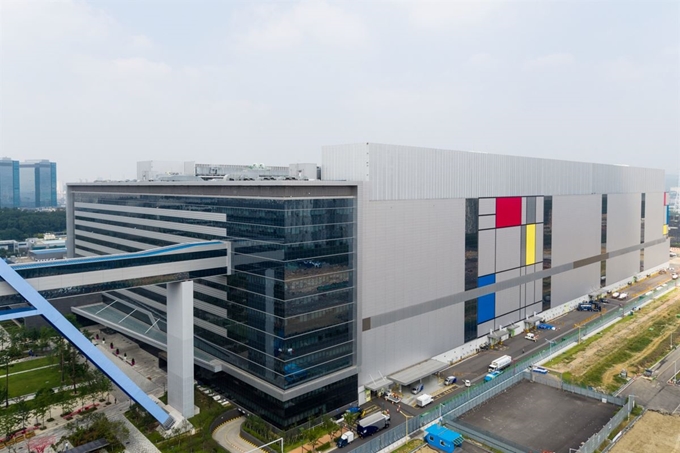
В сегодняшнем официальном пресс-релизе Samsung Electronics объявляет о старте массового производства своего первого коммерческого продукта со встроенной магнитной памятью с произвольной выборкой (eMRAM). В изделиях используется 28-нанометровый техпроцесс 28FDS, построенный на использовании полностью обеднённого кремния на изоляторе (FD-SOI). В аннотации подразделения Samsung Foundry говорится, что встраиваемой флэш-памяти (eFlash) присуще ограничение масштабируемости по той причине, что в основе лежит хранение заряда. Память eMRAM, работа которой основана на сопротивлении, выглядит многообещающим преемником eFlash, так как обеспечивает высокую масштабируемость и обладает такими преимуществами, как энергонезависимость, возможность произвольного доступа и высокая износостойкость. Представленное Samsung решение eMRAM по всем параметрам превосходт eFlash, включая скорость, уровень энергопотребления и более низкую стоимость. Поскольку в памяти eMRAM отсутствует цикл стирания перед размещением данных, скорость записи в этом случае примерно в 1.000 раз выше, чем у eFlash. Кроме того, eMRAM использует более низкие напряжения, чем eFlash. Ещё одним достоинством eMRAM является простая интеграция, требующая добавления меньшего количества слоёв. Это означает, что заказчики могут повторно использовать существующую инфраструктуру проектирования, снижая затраты. Ожидается, что память eMRAM, рассчитанная на изготовление по 28FD-SOI техпроцессу, найдёт применение в микроконтроллерах, микросхемах для интернета вещей (IoT) и искусственного интеллекта (AI). В течение года Samsung рассчитывает довести плотность eMRAM до 1 ГБ. Samsung Electronics Starts Commercial Shipment of eMRAM Product Based on 28nm FD-SOI Process Samsung's eMRAM will further strengthen the company’s technology leadership in embedded memory Samsung Electronics the world leader in semiconductor technology, today announced that it has commenced mass production of its first commercial embedded magnetic random access memory (eMRAM) product based on the company’s 28-nanometer(nm) fully-depleted silicon-on-insulator (FD-SOI) process technology, called 28FDS. As eFlash has faced scalability challenges due to a charge storage-based operation, eMRAM has been the most promising successor since its resistance-based operation allows strong scalability while also possessing outstanding technical characteristics of memory semiconductors such as nonvolatility, random access, and strong endurance. With today’s announcement, Samsung has proved its capability to overcome technical hurdles and demonstrated the possibility for further scalability of embedded memory technology to 28nm process node and beyond. Samsung’s 28FDS-based eMRAM solution offers unprecedented power and speed advantages with lower cost. Since eMRAM does not require an erase cycle before writing data, its writing speed is approximately a thousand times faster than eFlash. Also, eMRAM uses lower voltages than eFlash, and does not consume electric power when in power-off mode, resulting in great power efficiency. Furthermore, since an eMRAM module can easily be inserted in the back-end of the process by adding the least number of layers, it has less dependence on the front-end of the process for easy integration with existing logic technologies, such as bulk, fin, and FD-SOI transistor. With this plug-in module concept, customers can enjoy the benefit of reutilizing existing design infrastructure even with this added new technology, eMRAM, and saving costs at the same time. By combining with 28FD-SOI for better transistor control and minimizing leakage current through body-bias control, Samsung’s eMRAM solution will provide differentiated benefits for a variety of applications including micro controller unit (MCU), internet of things (IoT), and artificial intelligence (AI). “We are very proud of this achievement in offering right embedded non-volatile memory (eNVM) technology after overcoming complicated challenges of new materials.” said Ryan Lee, vice president of foundry marketing at Samsung Electronics. “By integrating eMRAM with existing proven logic technologies, Samsung Foundry continues to expand its eNVM process portfolio to provide distinct competitive advantages and excellent manufacturability to meet customers and market requirement.” A ceremony to celebrate this first shipment of eMRAM product will be held on March 6 at Samsung’s Giheung campus, Korea. Samsung plans to expand its options for high-density eNVM solutions, including a tape-out of 1Gb eMRAM test chip within this year.