Показаны сообщения с ярлыком FD-SOI. Показать все сообщения

пятница, 11 октября 2019 г.

Представлены новые микросхемы для автономных машин с ДВС и электромобилей на мероприятии Samsung Foundry Forum 2019 в Мюнхене


Для удовлетворения растущего спроса на рынках автономных авто и электромобилей Европы, Ближнего Востока и Африки Samsung предлагает чипы на основе техпроцессов 28 нм FDS и 14 нм

Samsung Electronics, мировой лидер в области передовых полупроводниковых технологий, представил расширенное портфолио инновационных микросхем для автомобильной промышленности Европы, Ближнего Востока и Африки.
Поскольку полупроводники в этом регионе востребованы в широком спектре отраслей, включая автомобилестроение, потребительскую электронику, сетевые технологии и Интернет вещей (IoT), Samsung представил ряд специализированных технологий, таких как FD-SOI, радиочастота (RF) и встроенная память, а также полный набор узлов процесса. Для повышения доступности полупроводниковых решений транснациональный гигант продемонстрировал инновационные платформы, которые объединяют ключевые технические элементы для развёртывания решений на базе 5G, IoT, высокопроизводительных вычислений (HPC) для создания «умных» автомобилей.
«В связи с активным развитием европейской автомобильной промышленности, рынок полупроводниковых решений для этой отрасли привлекает значительное внимание и, как ожидается, будет стремительно развиваться, чтобы удовлетворить растущий спрос в области автономных ДВС-машин и электромобилей», – отметил д-р И Эс Джанг (ES Jung), президент и глава направления производства полупроводников в Samsung Electronics.
Сейчас Samsung производит несколько полупроводниковых продуктов для автопрома, таких как помощник по вождению и информационно-развлекательные системы, в основном на базе 28-нанометровых (нм) FD-SOI и 14-нм техпроцессов. Для того, чтобы удовлетворить растущие запросы клиентов, Samsung планирует в ближайшем будущем представить решения на базе техпроцессов до 8 нм.
Samsung также уделяет особое внимание функциональной безопасности и надёжности компонентов, что имеет решающее значение в автомобильной промышленности, поскольку любой сбой может привести к аварии, травме или другим серьёзным последствиям. производитель уже доказал свою способность разрабатывать решения, соответствующие стандартам автомобильной индустрии, и получил сертификат ISO 26262 компании TÜV Rheinland, а также требованиям надёжности AEC-Q100 и системы управления качеством IATF 16969.

Samsung Introduces Advanced Automotive Foundry Solutions Tailored to EMEA Market at Samsung Foundry Forum 2019 Munich

To address the growing demand in the autonomous and electric vehicle market, Samsung offers various foundry solutions based on 28nm FDS and 14nm process

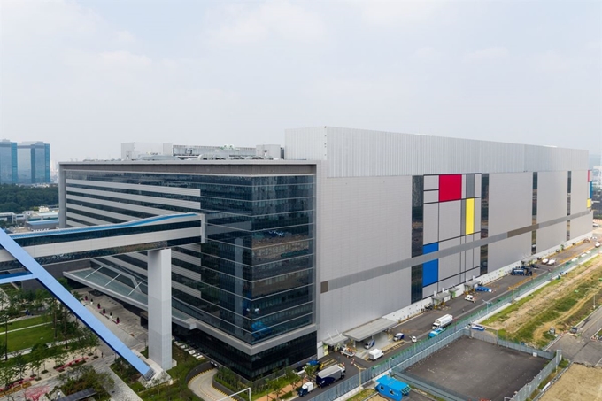
Samsung Electronics, a world leader in advanced semiconductor technology, today unveiled an expanded portfolio of cutting-edge foundry solutions at its Samsung Foundry Forum (SFF) 2019 Munich.
Samsung attracted more than 200 industry experts from fabless companies and foundry partners, and 16 partner booths displayed advanced foundry technology trends, a significant increase in both numbers compared to last year, representing a more solid customer base of Samsung Foundry as well as greater collaboration in Europe, Middle East, and Africa (EMEA).
Since the EMEA semiconductor market is in demand across a wide range of applications including automotive, consumer, network, and internet-of things (IoT), Samsung introduced various specialty technologies, such as FD-SOI, radio frequency (RF), and embedded memory along with comprehensive portfolio of foundry process nodes.
Samsung Electronics showcased its state-of-the-art foundry platforms that bring together essential technical elements for new-age applications, including 5G, IoT, automotive, and high performance computing (HPC), while expanding its design solution partners to improve global customers’ access to Samsung’s foundry solutions.
“It is a great honor to host our global foundry forum with increasing number of attendees every year. The forum has helped us work closely with our customers and strengthen Samsung’s foundry ecosystem,” said Dr. ES Jung, president and head of foundry business at Samsung Electronics, in the keynote speech. “We will strive to get more customer trust and be the best partner possible to prepare for the future with.”
Given the robustness of the European automotive industry, the foundry platform for automotive semiconductor market is drawing considerable attention, and is expected to rapidly grow to address the increasing demand in the autonomous and electric vehicle market.
Samsung is currently producing several automotive semiconductor products such as driving assistant and infotainment systems, mainly based on its 28-nanometer (nm) FD-SOI and 14nm process nodes. In order to respond to increasing customer inquiries, Samsung plans to expand its automotive process nodes to 8nm in near future.
Samsung is also focusing on functional safety and component reliability, which are critically important in the automotive industry, since any failure could cause serious consequences of accident or injury.
Samsung has already proven its ability to design IPs to meet the required automotive standard, and received the ISO 26262 certification for functional safety in automotive components from TÜV Rheinland. Complying with reliability standard AEC-Q100 and IATF 16969 quality management system, it is also preparing for automotive semiconductor production.
Meanwhile, in cooperation with ecosystem partners, Samsung will host its first SAFE™ (Samsung Advanced Foundry Ecosystem) Forum on Oct 17 in San Jose, to introduce Samsung’s IP, Electronic Design Automation (EDA), and packaging solutions in detail for foundry partners.

среда, 6 марта 2019 г.

Samsung Electronics объявляет о начале коммерческих поставок eMRAM


В сегодняшнем официальном пресс-релизе Samsung Electronics объявляет о старте массового производства своего первого коммерческого продукта со встроенной магнитной памятью с произвольной выборкой (eMRAM). В изделиях используется 28-нанометровый техпроцесс 28FDS, построенный на использовании полностью обеднённого кремния на изоляторе (FD-SOI).
В аннотации подразделения Samsung Foundry говорится, что встраиваемой флэш-памяти (eFlash) присуще ограничение масштабируемости по той причине, что в основе лежит хранение заряда. Память eMRAM, работа которой основана на сопротивлении, выглядит многообещающим преемником eFlash, так как обеспечивает высокую масштабируемость и обладает такими преимуществами, как энергонезависимость, возможность произвольного доступа и высокая износостойкость.
Представленное Samsung решение eMRAM по всем параметрам превосходт eFlash, включая скорость, уровень энергопотребления и более низкую стоимость. Поскольку в памяти eMRAM отсутствует цикл стирания перед размещением данных, скорость записи в этом случае примерно в 1.000 раз выше, чем у eFlash. Кроме того, eMRAM использует более низкие напряжения, чем eFlash.
Ещё одним достоинством eMRAM является простая интеграция, требующая добавления меньшего количества слоёв. Это означает, что заказчики могут повторно использовать существующую инфраструктуру проектирования, снижая затраты.
Ожидается, что память eMRAM, рассчитанная на изготовление по 28FD-SOI техпроцессу, найдёт применение в микроконтроллерах, микросхемах для интернета вещей (IoT) и искусственного интеллекта (AI).
В течение года Samsung рассчитывает довести плотность eMRAM до 1 ГБ.

Samsung Electronics Starts Commercial Shipment of eMRAM Product Based on 28nm FD-SOI Process

Samsung's eMRAM will further strengthen the company’s technology leadership in embedded memory

Samsung Electronics the world leader in semiconductor technology, today announced that it has commenced mass production of its first commercial embedded magnetic random access memory (eMRAM) product based on the company’s 28-nanometer(nm) fully-depleted silicon-on-insulator (FD-SOI) process technology, called 28FDS.
As eFlash has faced scalability challenges due to a charge storage-based operation, eMRAM has been the most promising successor since its resistance-based operation allows strong scalability while also possessing outstanding technical characteristics of memory semiconductors such as nonvolatility, random access, and strong endurance. With today’s announcement, Samsung has proved its capability to overcome technical hurdles and demonstrated the possibility for further scalability of embedded memory technology to 28nm process node and beyond.
Samsung’s 28FDS-based eMRAM solution offers unprecedented power and speed advantages with lower cost. Since eMRAM does not require an erase cycle before writing data, its writing speed is approximately a thousand times faster than eFlash. Also, eMRAM uses lower voltages than eFlash, and does not consume electric power when in power-off mode, resulting in great power efficiency.
Furthermore, since an eMRAM module can easily be inserted in the back-end of the process by adding the least number of layers, it has less dependence on the front-end of the process for easy integration with existing logic technologies, such as bulk, fin, and FD-SOI transistor. With this plug-in module concept, customers can enjoy the benefit of reutilizing existing design infrastructure even with this added new technology, eMRAM, and saving costs at the same time.
By combining with 28FD-SOI for better transistor control and minimizing leakage current through body-bias control, Samsung’s eMRAM solution will provide differentiated benefits for a variety of applications including micro controller unit (MCU), internet of things (IoT), and artificial intelligence (AI).
“We are very proud of this achievement in offering right embedded non-volatile memory (eNVM) technology after overcoming complicated challenges of new materials.” said Ryan Lee, vice president of foundry marketing at Samsung Electronics. “By integrating eMRAM with existing proven logic technologies, Samsung Foundry continues to expand its eNVM process portfolio to provide distinct competitive advantages and excellent manufacturability to meet customers and market requirement.”
A ceremony to celebrate this first shipment of eMRAM product will be held on March 6 at Samsung’s Giheung campus, Korea. Samsung plans to expand its options for high-density eNVM solutions, including a tape-out of 1Gb eMRAM test chip within this year.

вторник, 26 сентября 2017 г.

Samsung запускает производство чипов eMRAM по 28-нанометровой технологии FD-SOI


Подразделение по контрактному выпуску чипов Samsung Foundry, выделенное недавно в отдельное предприятие по инициативе материнской корпорации Samsung Electronics, уже готово начинать пробные отгрузки своей новейшей продукции заинтересованным клиентам.
Сегодня в официальном пресс-релизе Samsung Electronics опубликовано сообщение о достижении лидерских позиций южнокорейского вендора в развитии технологии FD-SOI. В производство запущен первый в отрасли чип eMRAM, рассчитанный на изготовление по 28-нанометровой технологии FD-SOI.
Ранее Samsung представил комплексную экосистему решений для создания продукции, рассчитанной на выпуск по этому техпроцессу, получившему обозначение 28FDS. Досрочная передача тестового чипа в производство не только подтверждает готовность техпроцесса к серийному выпуску — об этом производитель сообщил ещё в прошлом году, но и говорит о приверженности Samsung развитию технологии FD-SOI.
К передаче в производство по технологии FD-SOI уже подготовлены изделия более чем 40 заказчиков. Предполагается, что добавление возможности изготовления радиочастотных схем и памяти eMRAM с использованием техпроцессов 28FDS и 18FDS позволит Samsung привлечь дополнительных клиентов. Встраиваемая энергонезависимая память eMRAM характеризуется высоким быстродействием, низким энергопотреблением и высокой надёжностью.

Samsung Expands FD-SOI Process Technology Leadership and its Design Ecosystem Readiness

Samsung Foundry tapes out industry first eMRAM test chip based on 28nm FD-SOI process

Samsung Electronics, the world leader in advanced semiconductor technology, today announced it has expanded its differentiated FD-SOI process technology leadership by offering derivatives that include RF and eMRAM. Samsung already established a full set of FD-SOI design enablement solutions with key ecosystem partners for the 28-nanometer (nm) FD-SOI (28FDS) process technology. By accomplishing industry first eMRAM testchip tape-out milestone on 28FDS process technology, Samsung Foundry has demonstrated its 28FDS readiness with eMRAM technology leadership with the long commitment and expertise of Samsung’s semiconductor technology R&D capability.
“Samsung started mass production of its 28FDS process technology last year and reached the desired process maturity earlier than originally scheduled,” said Ryan Lee, Vice President of Foundry Marketing at Samsung Electronics. “So far we have taped out more than 40 products based on the FD-SOI process for various customers. With the addition of RF and eMRAM on 28FDS and 18FDS technologies, we expect an increasing number of product engagements.”
Samsung eMRAM is the newest addition to the family of embedded non-volatile memories and it offers unprecedented speed, power and endurance advantages.
“By adding only three layers in the back-end of the process, we can simply integrate the new eMRAM cells into the existing baseline FD-SOI process,” said Gitae Jeong, Senior Vice President of the Advanced Technology Development Team at Samsung Electronics. “Combined with Samsung’s memory technology leadership and its differentiated FD-SOI technology, we finally succeeded in incorporating eMRAM into various commercial applications”
“Samsung is working with NXP on a test chip to deliver eMRAM macro capability which is optimized for embedded processor integration and manufacturing.” said Ron Martino, VP and GM for NXP’s iMX Applications Processor product line. “This test chip is complete and will produce results in the 4th quarter. This work will further enable the vision of integrating diverse SOC components on a single SOC in a cost effective manner.”
Samsung has completed its full set of 28FDS technology eco-system solutions with various eco- system partners including Cadence and Synopsys. Customers can access Samsung certified 28FDS reference flows from Cadence and Synopsys along with application-specific IP offerings.
“Through our collaboration with Samsung, our mutual customers can access the 28FDS certified, comprehensive Cadence RTL-to-GDS reference flow,” said KT Moore, vice president, product management in the Digital & Signoff Group at Cadence. “The Cadence tools integrate the back-biasing and multi-bit flip-flop design optimization features included with the Samsung 28FDS process technology, enabling designers to quickly and easily develop high-quality SoCs with optimal power and performance.”
“Early joint collaboration on PDKs, reference flows and IP is a hallmark of the Samsung/Synopsys relationship,” said Michael Jackson, corporate vice president of marketing and business development for the Design Group at Synopsys. “For Samsung’s 28FDS, our mutual customers can design with confidence, knowing that it has been fully certified for Synopsys’ Design Platform and Design Ware® IP.
Details on the recent updates to Samsung Foundry’s cutting-edge process technology including FD-SOI technology roadmap and readiness will be presented at the Shanghai FD-SOI Forum on September 26th, 2017, by ES Jung, Executive Vice President and General Manager of Foundry Business at Samsung Electronics.