Показаны сообщения с ярлыком Image Sensor. Показать все сообщения

пятница, 9 апреля 2021 г.

Samsung сокращает разрыв с Sony на рынке мобильных камер


Samsung медленно, но верно, воплощает в жизнь своё намерение стать ведущим игроком на рынке датчиков изображения для смартфонов. По данным исследовательской компании Strategy Analytics, разработки южнокорейского техногиганта завоёвывают всё большую популярность среди производителей мобильных гаджетов, в то время как доля японских сенсоров изображения снизилась.
Эксперты приводят данные, согласно которым за 2020-й год подразделение Samsung LSI, специализирующееся на выпуске камер, увеличило свою долю до 29%, в то время как глобальные показатели Sony "просели" до 46%. Несмотря на то, что японский производитель по-прежнему занимает доминирующее положение, это для него является "тревожным звонком". Как отмечает Strategy Analytics, ранее соотношение составляло 20% у Samsung против 50% у Sony. Рыночные наблюдатели полагают, что изменения произошли по двум причинам: переориентация части крупных мобильных брэндов на компоненты Samsung и сокращение заказов от попавшей под американские санкции Huawei, которая часто использовала фотосенсоры Sony.
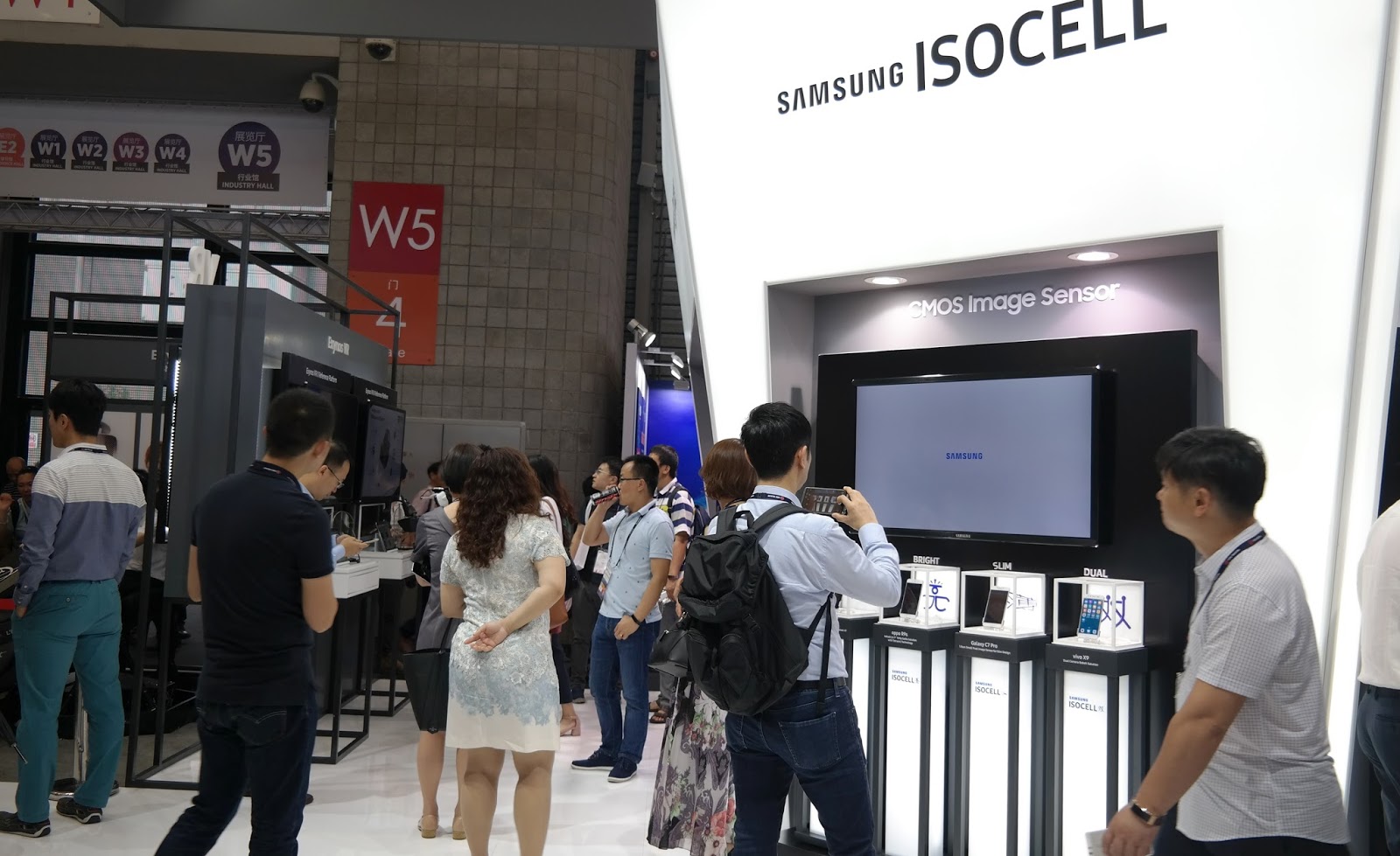
Samsung продолжает активно разрабатывать и выпускать новые датчики изображения. В феврале этого года вендор представил новый 50-мегапиксельный датчик ISOCELL GN2 с технологией автоматической фазовой фокусировки Dual Pixel Pro. Он предназначен для использования в смартфонах с продвинутой камерой. Размер пикселей в сенсоре составляет 1,4 микрометра. Он способен записывать видео в качестве Full HD с частотой 480 кадров в секунду, а 4K-видео — до 120 кадров в секунду. Кроме того, проектируются новые датчики с рекордным для отрасли разрешением в 200 и даже 600Мп. 

Samsung is expanding its presence in the mobile camera market

Traditionally, there is a tight competition between Samsung and Sony for making smartphone camera sensors, and both don’t want to leave behind. But it seems that Samsung is  getting closer to Sony and maybe could take it over in the next few years.
According to a report by Strategy Analytics, Sony currently holds a 46% share of the smartphone image sensor market. In the second position, Samsung LSI had a 29% in 2020.
Compared to previous years, Sony has lost its share and is losing it to its Korean rival. Sony used to have a 50% share of the market, but for 2020, it is slightly failing. On the other hand, Samsung is quietly taking over Sony’s share.
Samsung’s revenue share was below 20% years before, but now it has 29% of the global share. Thanks to the strategies and launching new sensors for mid-range to flagship smartphones, Samsung can even get more revenue shares. Samsung LSI is currently making ISOCELL camera sensors, and it’s doing a great job with them because the sensors made by them have always ranked at the top of smartphone camera rankings.
After Sony and Samsung, OmniVision Technologies holds 10% of the global revenue share. The remaining 15% is divided between other vendors.
An apparent reason for Sony’s loss is the U.S sanctions on Huawei. Sony has close ties with Huawei and is providing it with camera sensors. As one of the greatest OEMs in China, Huawei ships millions of units of smartphones each year. But U.S sanctions had a ruinous effect on Huawei’s operations and even made them enter new business segments. When Huawei sells fewer smartphones, this has a direct impact on Sony’s revenue as a partner.
Samsung also seized the opportunity and accelerated the sale of its sensors to other companies. Samsung is working on a variety of smartphone camera sensors. A few months ago, the company revealed a 108-megapixel ISOCELL HM3 camera sensor equipped with the latest technologies to capture sharper images.
The next camera sensor in Samsung’s lineup is ISOCELL GN2 that comes with interesting features, including dual-pixel autofocus and 5x optical zoom. Xiaomi is using this sensor at Mi 11 Ultra.
If you think a 108-megapixel sensor is enough for Samsung, you are entirely wrong because they’re working on a new generation of ISOCELL sensors with a 200 and even 600-megapixel resolution.

четверг, 3 мая 2018 г.

Samsung выпустил новый 16-Мп фотомодуль, позволяющий ускорить разработку мобильных устройств


Samsung представил новый 16-мегапиксельный датчик изображения ISOCELL Slim 3P9, который является решением типа Plug and Play (подключи и используй) и позволяет производителям мобильных гаджетов экономить несколько месяцев на разработке.
Суперкомпактный Samsung ISOCELL Slim 3P9 с 1-мкм пикселями и технологией Tetracell способен делать превосходные фото и видео, помещаясь даже в очень тонкие смартфоны. Благодаря технологии Tetracell, которая позволяет объединять сигнал 4-х соседних пикселей, новинка может работать как датчик изображения с пикселями размером 2 мкм для получения качественных снимков в условиях недостаточной освещённости.
В Samsung ISOCELL Slim 3P9 реализована новая версия системы фазового автофокуса, которая работает быстрее предшествующих моделей. Кроме того, датчик оснащён системой стабилизации, получающей данные от гироскопа, установленного в мобильном устройстве. Это существенно повышает чёткость фото и видео при съёмке с рук без использования дорогостоящих систем типа стэдикам.
Samsung ISOCELL Slim 3P9 уже доступен для заинтересованных производителей мобильной техники .

Samsung Makes Image Sensor Integration Easier with New 16Mp ISOCELL Slim 3P9 and Plug & Play Solution

Tetracell technology and 1.0μm pixel size enable sleekly designed smartphones to take more vivid pictures in darker environments

The ISOCELL Plug & Play solution can save up to four months of development time for manufacturers

Samsung Electronics, a world leader in advanced semiconductor technology, today introduced a new 16-megapixel (Mp) ISOCELL Slim 3P9 image sensor along with a Plug and Play solution, a pre-optimized turnkey camera module made up of an ISOCELL image sensor and preferred partner components to help expedite time-to-market.
“Samsung’s ISOCELL image sensors take advantage of various technologies to deliver innovative imaging experiences in mobile devices,” said Ben K. Hur, vice president of System LSI marketing at Samsung Electronics. “The ISOCELL Plug and Play solution will help reduce time-to-market for set makers and offer a quality-assured camera solution to end-users.”
The Samsung ISOCELL Slim 3P9 is a 1.0μm 16Mp image sensor with Tetracell technology that allows bright and vivid pictures in today’s sleekly designed smartphones. With Tetracell, a technology that merges four neighboring pixels, the 3P9 can function as a 2.0μm image sensor for front-facing cameras that can take brighter pictures in low-lit environments.
For faster auto-focusing, the 3P9 adopted an advanced phase detection auto-focus (PDAF) with doubled auto-focus agent density than that of conventional PDAF sensors. In addition, the sensor significantly stabilizes pictures and videos taken while in motion with a gyro-synchronizer that syncs frame exposure time from the sensor with movement data from the device’s gyroscope. Once the data is synced, the mobile processor can simply adjust the frames based on movement rather than rigorously analyzing each frame to detect and compensate for angular movement.
For easier camera optimization while accelerating time-to-market, Samsung also offers an ISOCELL Plug and Play solution for the 3P9 in a rear camera module. Optimizing a camera module, made up of parts from different providers, with the mobile processor can be an arduous and lengthy task for smartphone makers. Samsung’s ISOCELL Plug and Play solution simplifies this process by offering a turnkey ISOCELL sensor module tuned for Valued Camera eXperience (VCX)-grade image quality, along with other components, including lenses and actuators from preferred partners.
Since the optimization and reliability tests are done beforehand at the module-level rather than on the sensor alone, manufacturers can simply plug the camera module onto their device, saving up to four months of development time.
The Samsung ISOCELL Slim 3P9 with Plug and Play solution is currently available.

пятница, 16 марта 2018 г.

Samsung активно наращивает производство датчиков изображения, ослабляя позиции Sony


Конгломерат Samsung планирует существенно модернизирировать свои производственные линии, чтобы удвоить темпы выпуска датчиков изображения уже в текущем году и более эффективно конкурировать с Sony.
Как сообщает бизнес-портал The Investor со ссылкой на ETNews, модернизации подвергнется 13-я линия на заводе в городе Хвасон, где производятся модули оперативной памяти. Уже во второй половине 2018 года на ней начнут выпускать датчики изображения, о чём сообщают отраслевые источники. В прошлом году аналогичная модернизация была осуществлена и на 11-й линии этого завода, чтобы справиться с растущим спросом на датчики изображения. Процедура модернизации также завершится в этом году.
В прошлом году на указанных выше линиях Samsung произвёл 45.000 300-мм кремниевых подложек для датчиков изображения, а в этом году их производительность должна увеличиться до 120 тыс. единиц. Sony в этом году выпустит около 100.000 подложек для датчиков изображения. Таким образом, японская корпорация может потерять корону "короля фотоматриц".
Samsung намерен наращивать поставки новых датчиков изображения ISOCELL Fast 2L3, которые дебютировали во фламанских смартфонах Galaxy S9 и S9+, сторонним заказчикам (в основном китайским производителям мобильных девайсов). The Investor сообщает, что уже сейчас у южнокорейского техногиганта имеется более 10 заказчиков на эту продукцию.

Samsung ups the ante on image sensors

Tech giant Samsung Electronics plans to convert existing chip lines to double its image sensor production capacity this year in a bid to outshine its rival Sony, according to industry sources on March 15.
The Korean tech firm will transform its Line 13 plant for DRAM chips at the Hwaseong complex into one that produces image sensors in the second half of this year, an industry source close to the matter said.
Since last year, Samsung has been working on a project to switch the Line 11 DRAM plant in the complex into an image sensor line to meet its rising demand. The transformation is expected to be completed later this year. 
“The output of image sensors based on 300-millimeter wafers at the lines 11 and 13 can reach up to 120,000 units, up from 45,000 units of the 300mm wafers produced by the company last year,” the source said. 
The 120,000 also beats Sony’s estimated annual image wafer production capacity of 100,000 units. 
Aside from Sony, Samsung is the only company that commercialized three-layered image sensors stacking a logic chip and a DRAM chip on top of the sensor itself. Developed by Samsung’s system LSI business unit, the sensor enables the Galaxy S9 smartphone to shoot a slow-motion video at 960 frames per second.
Samsung is said to have more than 10 clients in the image sensor business, and it’s also reportedly in talks with global carmakers who are eager to install advanced camera sensors in cars for safety and security reasons.
While beefing up facilities for 300mm image sensor wafers, the Korean chip company plans to simultaneously scale down the production of 200mm wafers. Aiming to cushion the reduced DRAM production, it will additionally build new facilities at the Line 1 DRAM plant in Pyeongtaek and convert part of the Line 16 planar NAND flash memory chip plant in Hwaseong.

четверг, 12 октября 2017 г.

Samsung представил новые фотосенсоры с технологией ISOCELL для мобильных устройств и IoT-девайсов


Корпорация Samsung Electronics в официальном пресс-релизе объявила о выпуске сенсоров нового поколения. В них применяется фирменная технология изолирования фотодиодов каждого пикселя (ISOCELL) для уменьшения перекрёстных помех.
Новые датчики получили маркировку Fast 2L9 и Slim 2X7. Они предназначены для мобильных устройств и различных гаджетов Интернета вещей (IoT). Производитель отмечает малую толщину датчиков, позволяющую делать камеры, не выступающие из корпуса смартфона.
Fast 2L9 с разрешением 12Мп имеет пиксели размером 1,28 мкм. В нём реализована хорошо зарекомендовавшая сетя профессиональная технология Dual Pixel, позволяющая увеличить светосилу делать качественные снимки даже в тёмное время суток.
Slim 2X7 с разрешением 24Мп имеет пиксели размером всего 0,9 мкм. Его особенностью является технология Tetracell, позволяющая повысить качество изображения при съёмке в темноте за счёт объединения сигнала 4-х соседних пикселей. При нормальном освещении можно получать качественные изображения в полном разрешении.

Samsung’s New Image Sensors Bring Fast and Slim Attributes to Mobile and IoT Applications

Samsung releases ISOCELL Fast 2L9 with Dual Pixel technology and ISOCELL Slim 2X7 with Tetracell technology
Samsung Electronics, a world leader in advanced semiconductor technology, today introduced two new ISOCELL image sensors: 1.28-micrometer (μm) 12-megapixel (Mp) ISOCELL Fast 2L9 with Dual Pixel technology, and ultra-small 0.9μm 24Mp ISOCELL Slim 2X7 with Tetracell technology.
Samsung ISOCELL image sensors fall into four categories—Fast, Slim, Bright and Dual—depending on their key attributes. As market demand for sleeker smartphones with advanced features increases, ISOCELL Fast 2L9 and Slim 2X7 both offer high resolution image sensors in small chip packages, delivering detailed pictures in low-light environments without a camera bump.
With Dual Pixel technology, the ISOCELL Fast 2L9 delivers ultra-fast auto-focus at a reduced pixel size from the previous Dual Pixel sensor’s 1.4μm to 1.28μm. Dual Pixel technology employs two photodiodes in each and every pixel of the sensor instead of only one. With 12 million focus detecting pixels, the sensor is able to not only quickly focus on small still objects, but also lock on and track moving objects without losing focus, even in low-light environments. With smaller pixel size, the ISOCELL Fast 2L9 can fit into slimmer camera modules, enabling bump-less designs for smartphones. Dual Pixel technology especially allows depth-of-field effect for taking bokeh, or aesthetically out-of-focused photographs, through a traditional single lens camera.
At 0.9μm, the ISOCELL Slim 2X7 is the first sensor in the industry to have the pixel size below 1.0μm. Even with such a small pixel size, the Slim 2X7 is able to provide high color fidelity with less noise due to the improved ISOCELL technology’s deeper DTI (deep trench isolation) that reduces color crosstalk and expands the full-well capacity to hold more light information. In addition, the small 0.9μm pixel size enables a 24Mp image sensor to be fitted in a thinner camera module, allowing premium smartphones to offer high resolution cameras in a very slim and elegant design.
The ISOCELL Slim 2X7 is also packed with Tetracell technology, which lets the sensor take brighter photographs in the dark and more detailed ones in well-lit environments. Tetracell improves performance in low-light situations by merging four neighboring pixels to work as one to increase light sensitivity. In bright environments, Tetracell uses a re-mosaic algorithm to produce full resolution images. This enables consumers to use the same front camera to take photos in various lighting conditions.
“Samsung ISOCELL Fast 2L9 and ISOCELL Slim 2X7 are new image sensors that fully utilize Samsung’s advanced pixel technology, and are highly versatile as they can be placed in both front and rear of a smartphone,” said Ben K. Hur, Vice President of System LSI Marketing at Samsung Electronics. “Samsung plans to further develop the Dual Pixel and 0.9μm-pixel product categories, and expand applicable devices for ISOCELL image sensors that can enhance photographing experiences for consumers.”

среда, 20 сентября 2017 г.

Эксперты предполагают, что камера Samsung Galaxy S9 превзойдёт возможности соперницы в iPhone X


Южнокорейский технопортал ETNews сообщает, что Samsung планирует осуществить прорыв в технологии создания матриц для мобильных устройств.
Новые матрицы для смартфонов Samsung будут способны сканировать изображение с рекордной скоростью 1000 кадров в секунду и по своим техническим параметрам вплотную приблизятся к возможностям дорогостоящих профессиональных решений, применяемых в телевещании.
Достигнуто это будет с помощью «трёхслойного датчика изображения», который будет конкурировать с последними разработками японской корпорации Sony. Смартфоны с подобными фотомодулями, применяемыми в таких моделях как Sony Xperia XZ, могут записывать эпизоды со сверхзамедленным движением.
ETNews утверждает, что подразделение Samsung Electromechanics заказало специальное оборудование, необходимое для запуска в производство новейших матриц. Пилотная партия должна быть выпущена уже в октябре текущего года, а с ноября начнётся серийный выпуск новых фотомодулей. В настоящее время в своих новейших флагманах южнокорейский техногигант использует двухслойные матрицы.
ETNews не раз доказывал, что является поставщиком достоверной информации, поэтому сомневаться в правдивости опубликованных сведений вряд ли возможно.
В статье также указывается, что в будущей трёхслойной матрице стековая технология TSV используется вместе с чипами памяти DRAM и другими полупроводниковыми элементами. Именно ячейки DRAM-памяти, служащие для временного хранения данных, позволяют добиться скорости считывания на уровне 1000 кадров в секунду.
По мнению специалистов, возможности камеры Samsung Galaxy S9 (именно в этом гаджете, предположительно, будет впервые применено новое решение) превзойдут параметры модулей Sony, используемых в самом дорогом "юбилейном" iPhone X, который выйдет только в ноябре. 
Как сообщается, Samsung будет использовать технологию стекинга TSV, а не термальную компрессию, чтобы избежать лишних затрат по лицензированию сторонних патентов.
В последнее время появилась информация, что Samsung ускорит выпуск следующего флагмана и представит его уже в январе 2018, а продажи, якобы, начнутся уже в начале февраля. Если это так, то iPhone X будет "царствовать" на мобильном Олимпе совем недолго.
Впрочем, никаких официальных комментариев на сей счёт представители Samsung традиционно не дают.

Samsung Electronics Developed Its Own Image Sensors That Can Take 1,000 Pictures in a Second

Samsung’s Smartphone camera is going to be developed to a standard that comes close to that of an expensive broadcasting equipment.
Reason being is because Samsung Electronics developed and is going to start mass-producing super-fast image sensor that can take up to 1,000 pictures in a second. With this sensor, Smartphone camera will be able to implement images such as ‘Slow Motion’ that is used to decide whether or not a referee made a correct decision in pro baseball. It is expected that Smartphone camera equipped with this sensor will be useful in capturing an object’s movement in detail such as fixing posture of a person who is swinging a golf club.
According to industries on the 17th, Samsung Electronics is going to start mass-producing ‘3-layered image sensor’ in November. This image sensor is made into a layered structure by connecting a system semiconductor (logic chip) that is in charge of calculations and DRAM chip that can temporarily store data through TSV (Through Silicon Via) technology. Samsung Electronics currently ordered special equipment for mass-production and is going to start mass-producing ‘3-layered image sensor’ after doing pilot operation in next month.
Image sensor that is used for current premium Smartphones is based on 2-layered structure that is composed of a sensor and a logic chip. If DRAM chip is added to this composition, a technology that rapidly can take up to 1,000 pictures in a second can be implemented.
3-layered structure was first commercialized by SONY, which is the top business in global markets for image sensors, earlier this year and it was used for SONY’s premium Smartphones such as Xperia XZ and XZ1 that were released this year. Micron’s 1Gb DRAM was added to SONY’s 3-layered structure.
SONY’s product inserts Micron’s DRAM chip between an image sensor and a logic chip. SONY established a batch process system that attaches a sensor, a DRAM chip, and a logic chip in a unit of a wafer. On the other hand, it is understood that Samsung Electronics is using a method that makes 2-layered structure with a sensor and a logic chip and attaches DRAM through TC (Thermal Compression) bonding method after flipping over a wafer. From productivity and production cost, SONY has an upper hand. It seems that a reason why Samsung Electronics decided to use its way is because it wanted to avoid using other patents.
SONY was the first in the world to develop 2-layered image sensor and 3-layered image sensor and is currently commercializing them. Late starters need to avoid using SONY’s patents. Due to this reason, only Samsung Electronics and OmniVision are the only ones so far that commercialized 2-layered image sensors let alone 3-layered image sensors. It is predicted that supply and demand of parts will be faster and more convenient for Samsung Electronics than SONY because Samsung Electronics can receive DRAMs internally.
Although TSV stacking technology can dramatically increase performance of a product, production cost also increases as well. Production cost goes even higher as all three chips have to be thrown away if one of them goes bad.
“Despite increase in production cost, major semiconductor industries continue to use TSV technology more frequently as value of increasing performance is higher than increased production cost.” said a representative in this industry.
It is predicted that Samsung Electronics’ 3-layered image sensors will be used for its next Galaxy Smartphones. Samsung Electronics’ Wireless Business Department has been receiving half of supply of image sensors from SONY and other half from Semiconductor Business Department. For example, it used its own image sensors for models that were released in South Korea and SONY’s image sensors for models that were released in the U.S. It is predicted that it will continue to use same plan for its next Smartphones.
However because this technology was first introduced through SONY’s Smartphones, it is unclear whether or not Wireless Business Department will actively advertise 3-layered image sensor as one of major technologies. On the other hand, iPhone X is able to take 240 pictures in a second based on full HD resolution.

среда, 28 июня 2017 г.

Samsung представил новое семейство датчиков изображений Isocell


Корпорация Samsung Electronics внедрила бренд Isocell для обозначения датчиков изображений. Соответствующее заявление южнокорейский гигант сделал на конференции Mobile World Congress (MWC) 2017, который проходит в Шанхае (Китай).
Isocell - это представленная в 2013 году технология, применяемая в камерах мобильных устройств Samsung. Isocell отделяет каждый пиксель физическим барьером, что уменьшает цветовые помехи, позволяет достичь улучшенной цветопередачи и обеспечивает высокое качество изображения даже при очень маленьком размере пикселей.
Линейка Samsung Isocell теперь включает 4 суб-брэнда: Bright, Fast, Slim и Dual. Первый обеспечивает яркое и чёткое изображение с насыщенной цветовой гаммой и низким уровнем шумов при слабой освещённости.
Isocell Fast - это быстрая автофокусировка на неподвижных и движущихся объектах, в том числе при съёмке при недостаточном освещении.
Isocell Slim имеет наименьший из представленных на рынке размер пикселей (около 0,9-1,0 мкм), что позволяет получать изображения высокого качества на самых тонких и компактных устройствах.
Isocell Dual - возможность совмещения на устройствах всех вышеперечисленных возможностей и соответствия требованиям к популярным сдвоенным камерам, говорится в официальном пресс-релизе вендора.

Samsung Introduces Image Sensor Brand ‘ISOCELL’ at 2017 MWC Shanghai

Samsung Electronics, a world leader in advanced semiconductor technology, today introduced its image sensor brand ‘ISOCELL®’ as well as demonstrated leading-edge solutions at the 2017 Mobile World Congress (MWC) Shanghai.
Samsung’s brand for its image sensor lineup is named after the company’s own ISOCELL technology, which is the optimum solution for today’s devices that require ultra-slim designs with high quality cameras. First introduced in 2013, ISOCELL technology separates each pixel with a physical barrier that reduces color crosstalk among pixels. This allows high color fidelity, enabling excellent image quality even with smaller pixels.
Samsung ISOCELL is underlined by four technological sub-brands—Bright, Fast, Slim and Dual—that respond to specific market demands:

*ISOCELL Bright sensors deliver bright and sharp images with high color fidelity and reduced noise in low light environments
*ISOCELL Fast sensors provide fast autofocus onto still or moving objects even when dark
*ISOCELL Slim sensors adopt the smallest pixel sizes available in the market at 0.9-1.0um, yet produce high quality images for the slimmest devices
*ISOCELL Dual sensors can be mixed and matched in various combinations on consumer devices to bring about features demanded in the latest dual camera trend

“Samsung ISOCELL is a brand that represents the essence of our leading pixel technologies. We expect the ISOCELL brand to help consumers easily acknowledge and confide in camera performance as well as overall quality of the device,” said Ben Hur, Vice President of System LSI marketing at Samsung Electronics. “With our advanced image sensor technologies, Samsung will continue to bring innovation to cameras used in smartphones and other applications.”
At MWC Shanghai, Samsung will be featuring advanced logic solutions, including the Exynos 9 series with 10-nanometer FinFET process technology, for a wide range of platforms such as mobile, Virtual Reality (VR) and wearable devices.