Показаны сообщения с ярлыком EUV. Показать все сообщения

пятница, 18 декабря 2020 г.

Samsung укрепляет позиции в сегменте контрактного производства чипов и сокращает разрыв с TSMC


Samsung Electronics заключает уже второй контракт на производство 8-нм графических чипов семейства Ampere по заказу NVIDIA. Предыдущее соглашение было заключено в сентябре уходящего года.
Вэб-портал газеты The Korea Economic Daily накануне сообщил о соглашении по новому контракту между Samsung и знаменитой американской компанией, чей головной офис находится в Санта-Кларе (штат Калифорния). Условия сделки не уточняются, но в пресс-релизе говорится о производстве 8-нм графических процессоров игрового назначения, а сумма контракта оценивается экспертами в сотни миллионов долларов США. Эта новость оказала положительное влияние на репутацию Samsung Electronics. В результате акции конкурирующей TSMC просели на 0,3 %, что означает первую, пусть и не очень значительную, реакцию рынка на возможный переход крупных заказчиков к Samsung в обозримой перспективе.
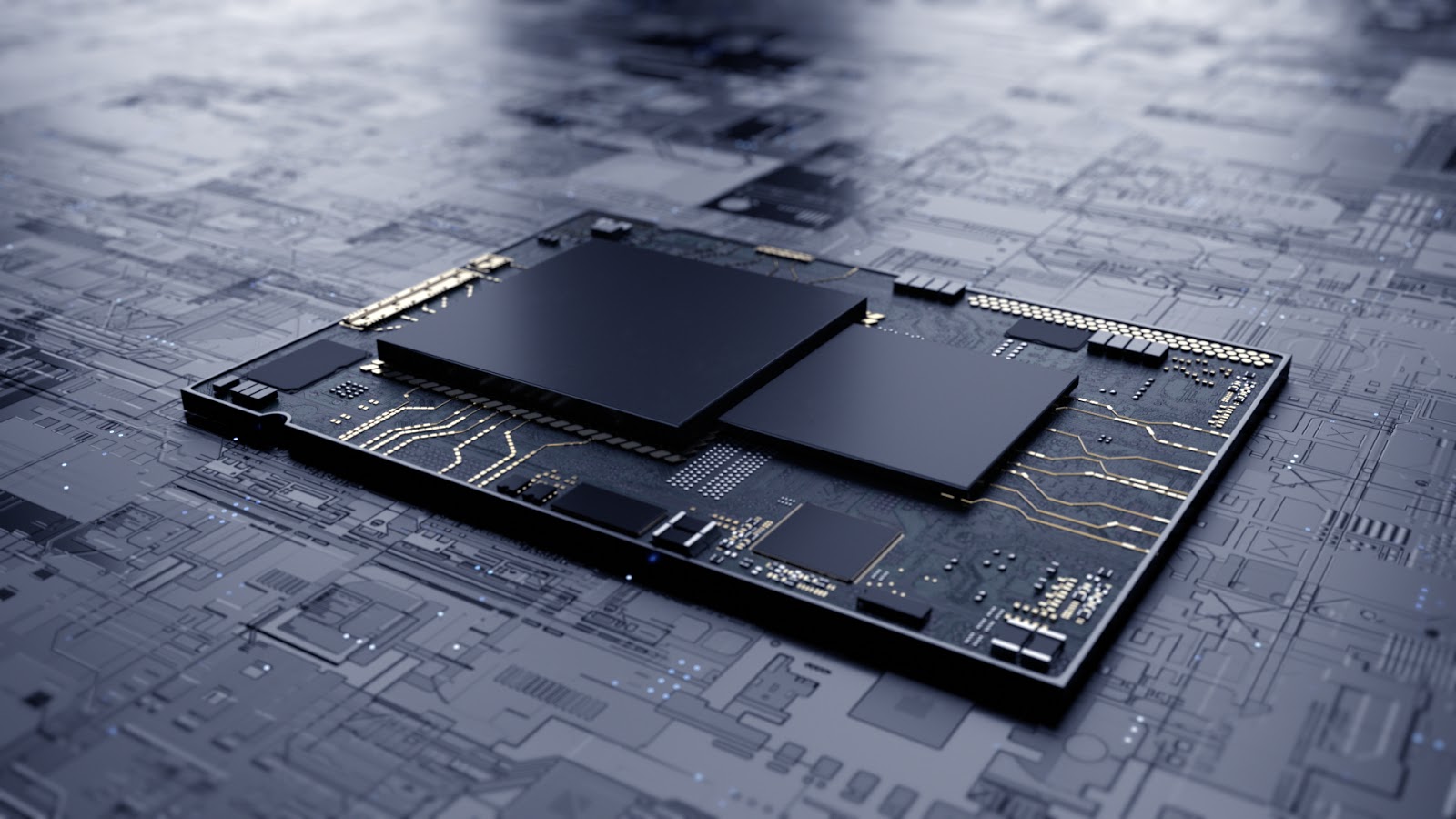
Южнокорейский электронный гигант будет выпускать графические процессоры NVIDIA на своём флагманском предприятии в Хвасоне. Возможно, новый контракт предусматривает увеличенные объёмы производства, и с его помощью NVIDIA постарается устранить дефицит видеокарт семейства GeForce RTX 30, который наблюдается уже несколько месяцев. Тем более, что на подходе мобильное семейство Ampere, и дополнительные мощности потребовались бы в любом случае.
По оценкам TrendForce, в этом году контрактный бизнес подразделения Samsung Foundry позволил увеличить выручку на 17,9 %, до $14,05 миллиарда. Помимо NVIDIA и Qualcomm, клиентами Samsung стали Google, IBM, Cisco и китайская Baidu. Мобильные чипы для Qualcomm корейский подрядчик тоже изготавливает по 8-нм технологии. Сейчас Samsung располагает семью производственными линиями для обслуживания сторонних заказчиков, которые расположены в Южной Корее и США. Доля техногиганта на мировом рынке контрактного производства чипов возросла до 16,4%.
В статье The Korea Economic Daily говорится, что Samsung не собирается останавливаться на достигнутом и будет расширять это направление за счёт ввода новых мощностей (в том числе  строительства очередного завода на производственном комплексе в Остине, США) и освоения более совершенных техпроцессов, включая 4-нм с использованием экстремального ультрафиолетового экспонирования (EUV). Это позволит значительно сократить отставание от TSMC в контрактном полупроводниковом бизнесе и привлечь новых клиентов.
По данным отраслевых источников, Samsung ежегодно тратит по 10 триллионов вон (8,6 миллиарда долларов) на разработку технологий производства микросхем и приобретение соответствующего оборудования.

Samsung clinches 2nd deal to make Nvidia’s latest gaming chips

Samsung Electronics Co. will manufacture Nvidia Corp.’s latest gaming chips in the second such contract of the year from the US chipmaker, as the South Korean tech giant aims to expand its presence in the foundry business.
Samsung, the world’s second-largest foundry player, has clinched a deal to make Nvidia’s next-generation graphic processing unit (GPU), the Ampere GeForce RTX30 series, using its 8-nanometer process technology, according to the semiconductor industry on Dec. 17.
The contract is Samsung’s second order this year from the Santa Clara, California-based company, following a similar deal in September.
The value of the latest deal is unknown but the industry estimates the contract is worth hundreds of billions of won. Samsung is expected to make the gaming chips at its Hwaseong plant.
Analysts said the contract is significant in that Samsung won the deal amid market talk that Nvidia’s new GPU has been in tight supply due to unsatisfactory 8 nm process yield rates at its foundry partner Samsung, raising speculation that the US company may award the contract to Taiwan Semiconductor Manufacturing Co. (TSMC), the industry leader.
Industry officials said Nvidia has favored Samsung over TSMC in consideration of Samsung’s technology and the need for quick delivery of the chips. The RTX3080, priced at $699, the same as its previous model, has been in high demand because of its faster data processing speed.
Samsung has been stepping up efforts to enhance its presence in the global foundry market as specialty DRAM prices are expected to continue their rally into next year amid tight supply.
Earlier this month, Samsung announced a leadership change in its two key businesses, memory chips and foundry, as part of its bid to gain further ground in the global chipmaking sector.
Analysts said Samsung’s new foundry chief Choi Si-young will be asked to narrow the gap with TSMC in coming years.
According to market researcher TrendForce, Samsung’s foundry business is expected to post a record $14.05 billion in sales this year, up 17.9% from 2019, as the company is expanding its client base beyond Nvidia to Qualcomm Technologies Inc., Google, IBM, Cisco and China’s Baidu.
In October, Samsung signed a deal to make mobile chips for Qualcomm, using its 8 nm technology.
To advance its technological leadership, Samsung has introduced an extreme ultraviolet (EUV) lithography technology for 7 nm and finer products.
“Through the more advanced 4 nm processing node, we’ll further narrow the gap with TSMC,” said Samsung’s foundry chief Choi.
More recently, Samsung has purchased a giant lot of land in Austin, Texas, where its US chip plant is located, raising expectations that the company may expand its foundry business.
Samsung is known to be spending 10 trillion won ($8.6 billion) a year to develop chip foundry technology and purchase related equipment to close in on its bigger rival TSMC.
Currently, Samsung operates seven foundry production lines in Korea and the US.
Samsung’s market share in the global foundry industry is estimated at 16.4% as of the fourth quarter of 2020, following TSMC’s 55.6, according to TrendForce.

пятница, 16 октября 2020 г.

Samsung Electronics расширяет сотрудничество с ASML в области EUV-литографии


Samsung несколько лет назад вложил сотни миллионов долларов в акции ASML, чтобы помочь европейскому холдингу с освоением производства литографических сканеров класса EUV. Другими крупными инвесторами были TSMC и Intel.
Как сообщает The Korea Times, Samsung пока не очень доволен развитием EUV-литографии на своих предприятиях, поэтому пришло время активизировать сотрудничество с ASML.
Такие выводы газета делает на основе комментариев, полученных от вице-председателя Samsung Electronics Ли Джэй-ёна (Lee Jae-yong) после его возвращения из недельной командировки в Нидерланды, где располагается штаб-квартира ASML. Сообщается, что топ-менеджер Samsung подтвердил цель своей поездки — поиск путей углубления сотрудничества при освоении процесса литографии со сверхжёстким ультрафиолетовым излучением (EUV).
На встрече в Нидерландах обсуждались вопросы покупки EUV-сканеров, а также содействия ASML в адаптации оборудования для производства микросхем памяти нового поколения. Ли-младший в ходе своей поездки посетил линию по производству EUV-сканеров ASML.
Интерес Samsung к закупкам оборудования ASML нового поколения обусловлен несколькими факторами. Во-первых, корпорация переводит на EUV-литографию производство микросхем памяти. Во-вторых, контрактное производство Samsung для сторонних заказчиков тоже нуждается в EUV-сканерах. Каждый новый техпроцесс требует всё более крупных капитальных затрат, поэтому Samsung не может оправдать расходы только за счёт производства чипов для собственных нужд. Кроме того, рынок памяти подвержен цикличным колебаниям, и Samsung намерен сократить периоды спада за счёт расширения более предсказуемого рынка контрактных услуг.
TSMC является главным клиентом ASML, но Samsung хочет добиться определённых преференций и для себя.
Один EUV-сканер стоит около $35 миллионов, поэтому чёткое планирование их поставок зависит от стабильного финансирования. На предприятии в Хвасоне Samsung собирается освоить выпуск продукции по 5-нм и более прогрессивным технологиям с применением EUV-литографии. Стремление электронного гиганта укрепить отношения с европейским поставщиком также обусловлено ростом напряжённости в отношениях между Южной Кореей и Японией.

Samsung Electronics expands cooperation with ASML in EUV lithography

Months after Samsung Electronics Vice Chairman Lee Jae-yong told President Moon Jae-in that the world's top memory chip manufacturer was working on developing extreme ultraviolet (EUV) scanner technology, he has confirmed that the company is in talks to advance its business relationship with ASML further.
"This time, I've been exploring ways to develop relations regarding EUV," Lee told reporters upon his arrival at Gimpo International Airport from the Netherlands, Wednesday. Lee went home after he tested negative for COVID-19.
In a statement, Samsung Electronics headquarters in Seoul said Lee met with top management at ASML including CEO Peter Wennink and CTO Martin van den Brink at their head office in Eindhoven, on the sidelines of his week-long trip.
The meeting covered various issues of mutual interest, such as ASML's plans to sell EUV equipment and the specifics of the two-way partnership's development of next-generation memory chips. The statement also said Lee toured EUV equipment manufacturing lines.
EUV equipment is vital for fabricating chips at the 7-nanometer node level and below. While an alternative fabrication method using multiple overlaid patterning iterations employing older deep ultraviolet (DUV) scanner technology is available to reduce pattern size, EUV technology has the upper hand in terms of better yield (defection rate). ASML has a high level of trust in that technology both in terms of intellectual property and cost.
After Japan delisted Korea from its list of most trusted business partners, President Moon encouraged Samsung and the country's other top manufacturers to invest in cutting their reliance for crucial industrial materials on imports from Tokyo. When Moon visited Samsung's new memory chip lines ― that will use EUV tech ― being built in the provincial city of Hwaseong, Lee said the decision was part of the company's strategy to better prepare for the future.
Amid the growing demand for logic- and custom-based memory semiconductors with the legacy memory chip market being saturated mostly due to the rise of Chinese companies, Samsung has been sharing its EUV tech knowhow with ASML. EUV is still pricey as the tools cost $35 million or more per system. The Korean company is also battling with its chief system chip rival TSMC in the heated foundry chips competition.
Samsung plans to manufacture EUV-based ultra-thin chips below 5 nanometers at its Hwaseong plant.

понедельник, 31 августа 2020 г.

Samsung запустил в массовое производство самую быструю и ёмкую память LPDDR5


Samsung Electronics объявляет о начале массового производства первых отрасли 16-Гб чипов памяти LPDDR5 для флагманских смартфонов нового поколения. Новая энергозависимая память на 16% быстрее образцов, применяемых в современных топовых гаджетах.

Новое поколение LPDDR5

Samsung приступил к массовому производству первых в отрасли мобильных чипов энергоэффективной  памяти LPDDR5 ёмкостью 16Гб, говорится в официальном пресс-релизе.
Помимо рекордной ёмкости,, заявлена самая высокая производительность изделия в своём классе. Предполагается, что новинка найдёт применение во флагманских смартфонах следующего поколения.
При заявленной скорости в 6400 Мбит/сек новинка примерно на 16% быстрее 12-Гб LPDDR5 (5500 Мбит/сек), которые применяются в большинстве современных флагманов. В упаковке 16Гб такая память, как отмечают в Samsung, может обеспечить передачу 51,2Гб информации (эквивалент 10 фильмов формата Full HD размером 5 Гб) за одну секунду.
Благодаря использованию техпроцесса 1z, упаковка LPDDR5 уменьшилась на 30% по сравнению с предшественником. Таким образом, в корпусе смартфонов на базе новой памяти производители смогут уместить больше компонентов. Упаковка ёмкостью 16Гб теперь состоит из 8-ми микросхем вместо прежних 12 с технологией 1y (8 чипов по 12Гб и 4 по 8 Гб).
В 2021 году. Samsung намерен укрепить своё положение в качестве поставщика памяти для мировых производителей смартфонов, а также увеличить долю на рынке LPDDR5 для автомобильной электроники за счёт решений с поддержкой работы в большом температурном диапазоне.

Вторая производственная линия в Пхёнтхэке

Выпуск кристаллов новой LPDDR5-памяти налажен на собственной (второй) производственной линии южнокорейской корпорации, которая расположена в Пхёнтхэке. Производство осуществляется в соответствии с техпроцессом 10нм (1z) 3-го поколения в крайнем ультрафиолетовом диапазоне (EUV, Extreme Ultraviolet).
Вторая производственная линия Samsung в Пхёнтхэке занимает площадь более чем 128.000 квадратных метров, что эквивалентно суммарной площади 16-ти футбольных полей. На сегодняшний день это крупнейшее полупроводниковое производство в мире. Помимо передовой DRAM, здесь планируют выпускать флэш-память V-NAND, которая применяется в твердотельных накопителях (SSD).
LPDDR5 – это относительно новый стандарт оперативной памяти для мобильных устройств, в частности смартфонов, планшетов и ноутбуков. Модули LPDDR (Low-power DDR) отличаются от DDR, в первую очередь, пониженным энергопотреблением.
Samsung стал первым в мире производителем, наладившим массовый выпуск 12-Гб мобильной DRAM-памяти LPDDR5. Конвейер заработал в июне 2019 г., и первые чипы имели объём 6Гб. Первые 12-Гб модули были выпущены в сентябре 2019 года. Они обеспечивали скорость передачи данных 5500 Мбит/cек при этом на 30% был снижен уровень потребления энергии по сравнению с предшественником (LPDDR4x).
В конце февраля 2020-го Samsung запустил в серию 16-Гб модули памяти на базе ранее представленных 12-Гб чипов с пропускной способностью 5500 Мбит/сек.

Samsung Begins Mass Production of 16Gb LPDDR5 DRAM at World’s Largest Semiconductor Line

Samsung starts shipping industry's first third-gen 10nm-class (1z) EUV-based 16Gb LPDDR5 DRAM. Following DRAM, new Pyeongtaek Line 2 to produce next-gen V-NAND and foundry solutions.

Samsung Electronics, the world leader in advanced memory technology, today announced that its second production line in Pyeongtaek, Korea, has commenced mass production of the industry’s first 16-gigabit (Gb) LPDDR5 mobile DRAM, using extreme ultraviolet (EUV) technology. Built on Samsung’s third-generation 10nm-class (1z) process, the new 16Gb LPDDR5 boasts the highest mobile memory performance and largest capacity to enable more consumers to enjoy the full benefits of 5G and AI features in next-generation smartphones.
“The 1z-based 16Gb LPDDR5 elevates the industry to a new threshold, overcoming a major developmental hurdle in DRAM scaling at advanced nodes,” said Jung-bae Lee, executive vice president of DRAM Product & Technology at Samsung Electronics. “We will continue to expand our premium DRAM lineup and exceed customer demands, as we lead in growing the overall memory market.”

Expanding Manufacturing Capacity in Pyeongtaek Complex

Spanning more than 128,900 square meters (over 1.3 million square feet) – equivalent to about 16 soccer fields – Samsung’s Pyeongtaek Line 2 is the largest-scale semiconductor production line to date.
The new Pyeongtaek line will serve as the key manufacturing hub for the industry’s most advanced semiconductor technologies, delivering cutting-edge DRAM followed by next-generation V-NAND and foundry solutions, while reinforcing the company’s leadership in the Industry 4.0 era.

Fastest, Largest-capacity Mobile Memory

Based on today’s most advanced (1z) process node, Samsung’s new 16Gb LPDDR5 is the first memory to be mass produced using EUV technology, providing the highest speed and largest capacity available in mobile DRAM.
At 6,400 megabits per second (Mb/s), the new LPDDR5 is about 16 percent faster than the 12Gb LPDDR5 (5,500Mb/s) found in most of today’s flagship mobile devices. When made into a 16GB package, the LPDDR5 can transfer about 10 5GB-sized full-HD movies, or 51.2GB of data, in one second.
Thanks to its use of the first commercial 1z process, the LPDDR5 package is 30 percent thinner than its predecessor, enabling 5G and multi-camera smartphones as well as foldable devices to pack more functionality into a slim design. The 16Gb LPDDR5 can build a 16GB package with only eight chips, whereas its 1y-based predecessor requires 12 chips (eight 12Gb chips and four 8Gb chips) to provide the same capacity.
By delivering the first 1z-based 16GB LPDDR5 package to global smartphone makers, Samsung plans to further strengthen its presence in the flagship mobile device market throughout 2021. Samsung will also expand the use of its LPDDR5 offerings into automotive applications, offering an extended temperature range to meet strict safety and reliability standards in extreme environments.

понедельник, 17 августа 2020 г.

Samsung представил новую технологию объёмной компоновки микросхем


Применение этой технологии позволяет масштабировать пропускную способность и плотность микросхем при создании современных приложений

Samsung Electronics, мировой лидер в области передовых полупроводниковых технологий представил технологию 3D-корпусирования микросхем, eXtended-Cube (X-Cube), предназначенной для использования с самыми современными технологическими процессами. Вместе с разработанной Samsung технологией сквозных отверстий через кремний (through-silicon, TSV), X-Cube обеспечивает значительный прирост в скорости и энергоэффективности, помогая удовлетворить строгие требования к производительности со стороны приложений следующего поколения, в том числе в области сетей 5-го поколения, искусственного интеллекта, высокопроизводительных вычислений, а также мобильной и носимой электроники.
«Новая технология трехмерной интеграции от Samsung обеспечивает надежные TSV-межсоединения даже при использовании самых современных технологических процессов на базе EUV-литографии, – говорит Мунсу Канг (Moonsoo Kang), старший вице-президент по стратегии полупроводникового рынка в Samsung Electronics. – Мы стремимся внедрять самые современные инновации в области объёмного корпусирования, чтобы раздвигать границы возможного в сфере полупроводниковых технологий».
С X-Cube от Samsung разработчики микросхем получают дополнительную гибкость при создании индивидуальных решений, наилучшим образом отвечающих их уникальным требованиям. В тестовом чипе X-Cube, построенном на базе 7-нм техпроцесса, используется технология TSV для размещения SRAM-памяти поверх логического кристалла, что позволяет высвободить место и размещать больше памяти при меньшей площади микросхемы. Благодаря трехмерной интеграции ультратонкая конструкция корпуса обеспечивает значительно более короткие пути прохождения сигнала между кристаллами для максимальной скорости передачи данных и энергоэффективности. Заказчики также могут масштабировать пропускную способность и плотность памяти в соответствии с заданными спецификациями.
Проверенная на кремнии методология и процессы проектирования Samsung X-Cube уже сегодня могут использоваться с современными техпроцессами, в том числе 7нм и 5нм узлами. Развивая свой исходный дизайн, Samsung планирует продолжить сотрудничество с глобальными заказчиками, не имеющими собственных производственных мощностей, по внедрению решений объёмной интеграции в новых высокопроизводительных приложениях следующих поколений.
Более подробная информация о технологии Samsung X-Cube будет представлена на ежегодной конференции по высокопроизводительным вычислениям Hot Chips, трансляция которой будет осуществляться в режиме реального времени 16-18 августа 2020 года.

Samsung Announces Availability of its Silicon-Proven 3D IC Technology for High-Performance Applications

Samsung 'X-Cube' enables industry-first 3D SRAM-logic working silicon at 7nm and beyond. Bandwidth and density can be scaled to suit diverse design requirements in emerging applications.

Samsung Electronics, a world leader in advanced semiconductor technology, today announced the immediate availability of its silicon-proven 3D IC packaging technology, eXtended-Cube (X-Cube), for today’s most advanced process nodes. Leveraging Samsung’s through-silicon via (TSV) technology, X-Cube enables significant leaps in speed and power efficiency to help address the rigorous performance demands of next-generation applications including 5G, artificial intelligence, high-performance computing, as well as mobile and wearable.
“Samsung’s new 3D integration technology ensures reliable TSV interconnections even at the cutting-edge EUV process nodes,” said Moonsoo Kang, senior vice president of Foundry Market Strategy at Samsung Electronics. “We are committed to bringing more 3D IC innovation that can push the boundaries of semiconductors.”With Samsung’s X-Cube, chip designers can enjoy greater flexibility to build custom solutions that best suit their unique requirements. The X-Cube test chip built on 7nm uses TSV technology to stack SRAM on top of a logic die, freeing up space to pack more memory into a smaller footprint. Enabled by 3D integration, the ultra-thin package design features significantly shorter signal paths between the dies for maximized data speed and energy efficiency. Customers can also scale the memory bandwidth and density to their desired specifications.
Samsung X-Cube’s silicon-proven design methodology and flow are available now for advanced nodes including 7nm and 5nm. Building on the initial design, Samsung plans to continue collaborating with global fabless customers to facilitate the deployment of 3D IC solutions in next-generation high-performance applications.
More details on Samsung X-Cube will be presented at Hot Chips, an annual conference on high-performance computing, which will be livestreamed Aug. 16-18.

пятница, 22 мая 2020 г.

Samsung Electronics запускает новую линию по выпуску полупроводников в южнокорейском Пхёнтхэке


Новая линия станет основной производственной базой 5-нм EUV-решений для 5G, высокопроизводительных вычислений и AI / Samsung запустит производство на линии во втором полугодии 2021г.

Samsung Electronics, мировой лидер в области передовых полупроводниковых технологий, объявил о планах по увеличению производственных мощностей на новой линии завода в Пхёнтхэке (Южная Корея), в целях удовлетворения растущего во всём мире спроса на решения c применением технологии EUV (литографии в глубоком ультрафиолете / extreme ultraviolet).
Основное внимание новой линии, строительство которой уже началось, будет уделено EUV-решениям, выполненных по 5-нанометровому и ещё более тонким техпроцессам. Линия будет играть ключевую роль в расширении использования корпорацией самых современных технологических процессов для множества решений текущего и следующего поколений, включая 5G, высокопроизводительные вычисления (HPC) и искусственный интеллект (AI). Запуск в эксплуатацию запланирован на вторую половину 2021 года.
«Новое предприятие расширит производственные мощности Samsung для 5-нм и более тонких техпроцессов и предоставит возможность оперативно удовлетворять растущий спрос на решения для высокопроизводительных вычислений, – отметил д-р Юнг (ES Jung), президент и глава полупроводникового бизнеса Samsung Electronics. – Мы по-прежнему привержены удовлетворению потребностей наших клиентов посредством активных инвестиций и привлечения новых кадров. Это позволит нам продолжать развиваться, при этом обеспечивая устойчивый рост полупроводникового производства Samsung».
Запустив массовый выпуск EUV-решений по 7-нм техпроцессу в начале 2019 года, Samsung недавно приступил к серийному изготовлению чипов для EUV на новой линии в Хвасоне (Южная Корея). Ожидается, что с началом полной эксплуатации нового завода в Пхёнтэке в 2021 году, мощность производства EUV-решений Samsung значительно возрастёт.
Samsung намерен запустить массовое производство EUV-решений по 5-нм техпроцессу на заводе в Хвасоне во второй половине этого года. С учётом объекта в Пхёнтхэке у Samsung будет, в общей сложности, 7 линий по производству полупроводников в Южной Корее и США, в том числе 6 с использованием 12-дюймовых подложек и одна с использованием 8-дюймовых подложек.

Samsung Electronics Expands its Foundry Capacity with A New Production Line in Pyeongtaek, Korea

New line will become core manufacturing base for 5G·HPC·AI solutions with 5nm EUV / Samsung began construction this month for volume production in 2H 2021

Samsung Electronics, a world leader in advanced semiconductor technology, announced plans to boost its foundry capacity at the company’s new production line in Pyeongtaek, Korea, to meet growing global demand for cutting-edge extreme ultraviolet (EUV) solutions.
The new foundry line, which will focus on EUV-based 5 nanometer (nm) and below process technology, has just commenced construction this month and is expected to be in full operation in the second half of 2021. It will play a pivotal role as Samsung aims to expand the use of state-of-the-art process technologies across a myriad of current and next generation applications, including 5G, high-performance computing (HPC) and artificial intelligence (AI).
“This new production facility will expand Samsung’s manufacturing capabilities for sub-5nm process and enable us to rapidly respond to the increasing demand for EUV-based solutions,” said Dr. ES Jung, President and Head of Foundry Business at Samsung Electronics. “We remain committed to addressing the needs of our customers through active investments and recruitment of talents. This will enable us to continue to break new ground while driving robust growth for Samsung’s foundry business.”
Following the initial mass production of the EUV-based 7nm process in early 2019, Samsung recently added a new EUV-dedicated V1 line in Hwaseong, Korea, to its global foundry network. With the new Pyeongtaek facility starting full operation in 2021, Samsung’s foundry capacity based on EUV is expected to increase significantly.
Samsung is scheduled to start mass production of 5nm EUV process in the Hwaseong fab in the second half of this year.
With the addition of the Pyeongtaek fab, Samsung will have a total of seven foundry production lines located in South Korea and the United States, comprised of six 12-inch lines and one 8-inch line.

среда, 25 марта 2020 г.

Samsung отгрузил миллион первых в отрасли чипов EUV DRAM


Samsung Electronics объявляет о производстве и отгрузке 1 миллиона модулей первой на рынке памяти (D1x) DDR4 (Double Date Rate 4) DRAM, произведённых с использованием технологии EUV (литографии в глубоком ультрафиолете). Модули прошли валидирование крупнейших международных производителей электроники, и теперь вендор с их помощью сможет создавать инновационные функциональные узлы с использованием EUV для применения в премиальных ПК, мобильных устройствах, корпоративных серверах и центрах обработки данных.
Samsung первым применил технологию EUV в производстве DRAM-модулей, чтобы преодолеть ограничения по масштабированию этого типа чипов. Литография в глубоком ультрафиолете сокращает количество повторяющихся шагов при создании нескольких шаблонов и повышает точность их формирования. Это обеспечивает повышенную производительность и более высокий выход, а также сокращённое время разработки.
Технология EUV будет полностью развёрнута в будущих DRAM от Samsung, начиная с 4-го поколения 10-нм класса (D1a) или продвинутого 14-нм класса DRAM. Корпорация намерена начать серийное производство DDR5 и LPDDR5 на базе D1a в следующем году, что удвоит производительность 12-дюймовых пластин D1x.
В связи с расширением рынка DDR5/LPDDR5 в 2021 году Samsung продолжит укреплять сотрудничество с ведущими IT-клиентами и поставщиками полупроводников с целью оптимизации стандартных спецификаций, поскольку это ускорит переход к DDR5/LPDDR5 на всём рынке памяти.

Samsung Announces Industry’s First EUV DRAM with Shipment of First Million Modules

EUV-based 1st-gen 10nm-class DRAM (D1x) has completed its customer evaluations;
EUV to be fully deployed from 4th-gen 10nm-class DRAM (D1a) next year

Samsung Electronics, the world leader in advanced memory technology, today announced that it has successfully shipped one million of the industry’s first 10nm-class (D1x) DDR4 (Double Date Rate 4) DRAM modules based on extreme ultraviolet (EUV) technology. The new EUV-based DRAM modules have completed global customer evaluations, and will open the door to more cutting-edge EUV process nodes for use in premium PC, mobile, enterprise server and datacenter applications.
“With the production of our new EUV-based DRAM, we are demonstrating our full commitment toward providing revolutionary DRAM solutions in support of our global IT customers,” said Jung-bae Lee, executive vice president of DRAM Product & Technology at Samsung Electronics. “This major advancement underscores how we will continue contributing to global IT innovation through timely development of leading-edge process technologies and next-generation memory products for the premium memory market.”
Samsung is the first to adopt EUV in DRAM production to overcome challenges in DRAM scaling. EUV technology reduces repetitive steps in multi-patterning and improves patterning accuracy, enabling enhanced performance and greater yields as well as shortened development time.
EUV will be fully deployed in Samsung’s future generations of DRAM, starting with its fourth-generation 10nm-class (D1a) or the highly-advanced 14nm-class, DRAM. Samsung expects to begin volume production of D1a-based DDR5 and LPDDR5 next year, which would double manufacturing productivity of the 12-inch D1x wafers.
In line with the expansion of the DDR5/LPDDR5 market next year, the company will further strengthen its collaboration with leading IT customers and semiconductor vendors on optimizing standard specifications, as it accelerates the transition to DDR5/LPDDR5 throughout the memory market.
To better address the growing demand for next-generation premium DRAM, Samsung will start the operation of a second semiconductor fabrication line in Pyeongtaek, South Korea, within the second half of this year.

воскресенье, 5 января 2020 г.

Samsung инвестирует $116 миллиардов в контрактное производство чипов


Samsung Electronics активно инвестирует в бизнес в области услуг контрактного производства чипов, чтобы конкурировать с тайваньской TSMC, сообщает информационное агентство Bloomberg.
В ближайшие 10 лет Samsung намерен инвестировать порядка 116 миллиардов долларов на контрактное производство полупроводниковой продукции. $64 миллиарда будут потрачены на исследования и разработки (R&D), а оставшиеся $69 миллиардов пойдут на расширение производственных мощностей, что позволит создать 15.000 рабочих мест.
Одно из направлений для инвестиций - процесс экстремальной ультрафиолетовой литографии (EUV, Extreme Ultraviolet Lithography). Его использование должно помочь южнокорейскому гиганту освоить 5-нм, 3-нм и более тонкие технологические процессы.
По оценкам TrendForce, в октябре-декабре 2019 года оборот контрактного подразделения Samsung Foundry вырос на 19,3% в годовом исчислении и достигнет 3,47 миллиарда долларов США.
Несмотря на впечатляющий рост, Samsung пока ещё значительно уступает TSMC. В 4-м квартале 2019 года выручка TSMC достигла 10,25 миллиарда долларов, что на 8,6% выше прошлогоднего результата. Тройку лидеров рынка фаундри-услуг традиционно замкнет GlobalFoundries с выручкой в 1,56 миллиарда долларов (+0,1%).

Samsung invests $ 116 billion in contract manufacturing chips

Bloomberg, 22/12/2019

Technology giants are increasingly designing their own semiconductors to optimize everything from artificial intelligence tasks to server performance and mobile battery life. Google has the Tensor Processing Unit, Apple Inc. has the A13 Bionic and Amazon.com Inc. has the Graviton2. What the titans all lack, however, is a factory to build the new chips they are dreaming up.
Enter Samsung Electronics Co., which is planning a decade-long, $116 billion push for their business. The South Korean company is investing heavily in the next step in miniaturizing semiconductors, a process called extreme ultraviolet lithography (EUV). It’s by far the priciest manufacturing upgrade Samsung has ever attempted, a risky bid to move beyond its established business of cranking out commoditized silicon and to leapfrog the incumbent leaders in the $250 billion foundry and logic-chip industry.
“A new market is opening up,” Yoon Jong Shik, executive vice president of Samsung’s foundry business, said at a forum recently held in Seoul. “Companies like Amazon, Google and Alibaba, which lack experience in silicon design, are seeking to make chips with their own concept ideas in order to boost their services. I think this would bring a significant breakthrough for our non-memory chip business.”
Samsung is a relative underdog in this growing field. The foundry business - as the manufacturing of chips for companies like Google and Qualcomm Inc. is known - is dominated by Taiwan Semiconductor Manufacturing Co. with more than half the market, according to TrendForce Corp. data that puts Samsung at 18%.
TSMC also took over Apple’s A-series processor manufacturing from Samsung, which was the original production partner. Samsung plans to spend about $10 billion per year on equipment, research and development over the next decade, but TSMC is even more ambitious with capital expenditure of around $14 billion for this year and next.
“It is not just a matter of willingness,” said CW Chung, head of pan-Asia technology at Nomura Financial Investment Co., in assessing Samsung’s chances of success. “Chip-making is like a composite art. Unless there are enough supports for all-round social infrastructures, it’d be a scarcely achievable goal.”
To win over clients, top Samsung executives are touring major cities from San Jose to Munich to Shanghai, hosting foundry forums and negotiating deals. ES Jung, president and general manager for the foundry business, is the frontman delivering Samsung’s “can-do” spiel at every gathering, where his practiced joke is to suggest that his initials stand for “engineering sample.”
“The complexity of the lines drawn by the EUV equipment is similar to building a spaceship,” said Jung while unveiling a $17 billion EUV plant in Hwaseong earlier this year, flanked by Samsung heir and de-facto boss Jay Y. Lee and South Korean President Moon Jae-in. The fab is planned to start mass production in February 2020.
A single EUV machine from ASML Holding NV costs $172 million and Samsung is setting up dozens of them in Hwaseong in an effort to be first with the technology. TSMC and Samsung are both expected to reach 5-nanometer production processes with EUV in the new year, which means they’ll have only each other to compete with in a market that’s only set to expand. And once they ramp up and achieve economies of scale, the overall process cycle time is likely to decrease by 20% and the foundry capacity output will increase by 25%, according to a Citigroup Inc. research report.
“TSMC is too busy with orders pouring in for new products as we enter into the 5G era,” said Greg Roh, senior vice president at Hyundai Motor Securities. “For Samsung, that’s bringing a good chance to expand their market share by offering lower prices and delivery schedules to meet clients’ needs.”
Samsung is collaborating with major clients on designing and manufacturing custom chips and that work is already starting to add to its revenue, according to one Samsung executive who has direct knowledge of the matter. The push toward bespoke processors in Silicon Valley and China is opening up fresh opportunities and Samsung already has established relationships, as demonstrated by its recent announcement that it’ll produce an AI chip for Baidu Inc. early next year.
Officials at Samsung believe the company has a competitive edge from its experience building both the chips and the devices that they go into. It is thus able to foresee and address the engineering requirements of its clients. Samsung believes its other trump card is an ability to package memory and logic chips into a single module, improving power and space efficiency. Analysts do warn, however, that some companies are wary about outsourcing production to a direct competitor in the consumer electronics market - lest Samsung learns and copies their chip designs in its own products.
“Ultimately, the success of Samsung’s logic chip business depends on its market positioning,” Hsu said. “On the foundry side, Samsung needs to eliminate its clients’ suspicions of Samsung LSI being a potential competitor.”
Samsung is reaching out to smartphone-making rivals and has already agreed to sell 5G Exynos chips to Vivo. At the same time, it’s going to be manufacturing Qualcomm’s 5G mobile chipset using the same EUV process. On yet another front, the company is competing with foundry customer Sony Corp. in the growing market for image sensors, having this year unveiled an unprecedented 108-megapixel camera for smartphones. “I think Samsung’s CMOS image sensor business will continue to do well, riding on the industry boom,” said Bloomberg Intelligence analyst Anthea Lai.
If Samsung can move ahead technologically, it should find no shortage of customers for its varied semiconductor offerings. Though China is increasingly turning to domestic suppliers for all things tech, the greater efficiency of EUV chips may be key in helping Samsung solicit business from the world’s second-biggest economy.
“The increased demand for in-house chips spells good news for the growth of the foundry industry,” TrendForce analyst Chris Hsu said.

четверг, 21 ноября 2019 г.

В Samsung разработали способ повышения эффективности EUV-литографии


Год назад мы сообщали, что Samsung первым в мире приступил к использованию сканеров диапазона EUV (13,5 нм) для коммерческого выпуска чипов. Можно сказать, что Samsung дал EUV-литографии путёвку в жизнь, хотя это не избавило её от "детских болезней", которые необходимо преодолеть. Проблем с EUV (Extreme Ultraviolet) довольно много и их необходимо решать параллельно развёртыванию всё новых и новых коммерческих систем. Samsung, являясь пионером в продвижении этой технологии, тщательно анализирует все возникающие трудности и постепенно находит пути для их преодоления.
На прошедшей 19 ноября конференции «The Korean Society of Semiconductor & Display Technology» в Университете Ханьян представитель Samsung рассказал о двух серьёзных проблемах, которые приходится решать по мере снижения масштаба технологического процесса при выпуске полупроводников. Одна проблема кроется в высокой плотности энергии пучка EUV-излучения, а вторая, связанная с ней ― в невозможности эффективно протравить тончайшие дорожки после обработки пластины и в сложностях с депонированием добавок в предельно узкие канавки цепей в кристаллах.
Высокая удельная плотность энергии EUV-луча ― в 10 раз больше, чем у луча 193-нм лазера ― ведёт к возникновению паразитных образований в фоторезисте, что вместе со ставшими более тонкими дорожками приводит к появлению так называемых микромостов. Иначе говоря, возникают не предусмотренные схемой перемычки, которые могут вызвать отказ микросхем. Сегодня корпорация борется с микромостами при помощи повторяемой кратковременной экспозиции и повторным травлением. При этом удлиняется производственный цикл, что только усугубится после очередного уменьшения масштаба технологических норм. Сканеры EUV ― это весьма дорогие установки стоимостью $171 миллион за штуку. Окупить такую установку очень тяжело и удлинение технологических циклов не будет этому способствовать.
Вторая проблема при использовании EUV-сканеров связана с уменьшением размеров элементов на кристалле. Канавки для цепей и элементов становятся уже, что затрудняет внесение примесей в полупроводники и даже циркуляцию химических составов в процессе травления. Чтобы протравить канавку, необходимо больше времени, реагентов и защитного покрытия в тех местах, которые не подлежат травлению.
Для устранения этих препятствий Samsung предлагает сделать две вещи. Во-первых, экстремально снизить рабочую температуру внутри камеры с обрабатываемой пластиной. Во-вторых, значительно понизить давление внутри камеры. Охлаждение до низких температур уменьшит активность реагентов и даст возможность избежать как появления микромостов (за счёт снижения чувствительности фоторезиста), так и снизит нагрузку на защитную полимерную плёнку. Низкое давление в камере, в сочетании с интенсивной обработкой протравленных зазоров рабочими газами для депонирования, усилит циркуляцию материалов в канавках и ускорит циклы травления и депонирования. Но пока это только теория, которую ещё предстоит довести до коммерческой реализации, сообщает южнокорейский технопортал ETNews.

Samsung Electronics Looks for Solutions on Two Challenges of EUV Process

EUV (Extreme Ultraviolet) process is the technology that is currently drawing the most interests for microfabrication process of semiconductor. However, there are still many tasks that need to be resolved as EUV process is still in its initial phase. Samsung Electronics stated that it is conducting R&D on various solutions such as extreme low-temperature process and extreme low-pressure process to resolve possible challenges.
Master Park Jong-cheol of Samsung Electronics explained during ‘The Korean Society of Semiconductor & Display Technology Fall Conference’, which was held at Hanyang University on the 19th, that there are currently two obstacles for etching process that shaves off circuits as the semiconductor industry is starting to enter an EUV process era.
‘Micro bridge’ that occurs at the bottom of a circuit is the first obstacle. Also, it has also become more difficult to place a material deep inside in order to shave off circuits as the width of a circuit has become extremely narrow.
EUV process is a photolithography process that repeatedly prints circuits on a circular wafer with EUV light source (13.5nm). Because the wavelength is about 14 times smaller than the wavelength of ArF (Argon Fluoride, 193nm) light source, which is the most commonly used light source, EUV process can print circuits more elaborately and finely. This is the reason why Samsung Electronics and TSMS from Taiwan are focusing all of their abilities in order to gain leadership in this technology.
However, shorter wavelength causes new flaws such as micro bridge.
EUV photoresist is applied on a semiconductor wafer during photolithography process. Main problem is that the energy of the wavelength of EUV light source becomes 10 times greater as wavelength becomes shower. Because wavelength and energy are inversely proportional, wavelength hits the surface of a wafer harder as it becomes shorter. Light source with greater energy either causes the nucleus of an atom of a reactant that is included in an EUV photoresist to pop out or it causes brand new atoms to combine. As a result, foreign substances that semiconductor manufacturers do not want are formed. In addition, the width of a circuit has become thinner causing areas that are not supposed to be shaved off to be connected. This is called micro bridge.
“Although photolithography process can be lengthened in order to resolve micro bridge issue, we have to consider the fact that the productivity of an EUV photolithography system that costs about $171 million (200 billion KRW) can decline faster.” said Master Park.
He explained that Samsung Electronics has chosen a method that repeatedly shaves off micro bridges while protecting the upper part of a circuit with polymer.
“Because it may be difficult to maintain this method for next-generation processes, it is likely that we are going to need a brand new etching technology.” said Master Park.
Another problem is that it has become difficult to place materials that are needed for etching process deep inside of a circuit as the width of a circuit has become significantly narrower. Polymer covers the surface during etching process in order to prevent circuits from shaved off unevenly.
Problem is that circuits made through EUV are already thin and that polymer that is currently used makes entrance even narrower and causes ‘bottleneck phenomenon’. As a result, more time and cost are necessary in order to place etching materials and ions deep inside through a narrow entrance.
“Because etching process time becomes longer and there needs to be more power to place etching materials deep inside, there is a vicious cycle such as protecting the upper part of a circuit even more.” said Master Park. “Samsung’s executive team is already aware of this issue and is laboring over for a solution.”
Master Park suggested ‘extreme low-temperature’ etching process as a possible solution. By decreasing the temperature of the inside of a chamber where wafers go in, gaseous movements that are necessary for etching process are minimized even without polymer. His solution is based on a principle that materials that are active in room temperature move slowly in extreme low-temperature.
“Extreme low-temperature method to create effective etching materials and ‘high pumping’ etching technology that prevents bottleneck phenomenon by forcing gas inside of a chamber to move faster can be possible alternatives.” said Master Park. “Samsung Electronics is currently conducting R&D on these technologies to apply them to actual mass-production process.” He also added that more research on these issues by the academic industry will be a big help for the semiconductor industry.

среда, 17 апреля 2019 г.

Samsung объявляет о завершении разработки технологии изготовления чипов по 5-нм техпроцессу, заметно опередив конкурентов


Samsung активно использует своё преимущество как первопроходца полупроводниковой литографии с применением сканеров EUV-диапазона. Пока конкуренты из TSMC только готовится начать использовать сканеры с длиной волны 13,5нм, адаптировав их для выпуска чипов в рамках второго поколения техпроцесса с нормами 7 нм, Samsung идёт дальше и заявляет о завершении разработки техпроцесса с проектными нормами 5нм. Более того, южнокорейский техногигант объявил о начале приёма заказов на выпуск 5-нм решений для производства на мультипроектных пластинах. Это означает, что Samsung готов принимать цифровые проекты чипов с указанными нормами и выпускать опытные партии рабочего 5-нм кремния.
Быстро перейти от предложения 7-нм техпроцесса с EUV на производство 5-нм решений (также с EUV) мэйджору отрасли помогло то обстоятельство, что Samsung сохранил совместимость проектных элементов (IP), инструментов проектирования и контроля. Кроме прочего это означает, что клиенты сэкономят средства на приобретение средств проектирования, тестирования и готовых IP-блоков. Наборы PDK для проектирования, методология (DM, design methodologies) и платформы автоматического проектирования EDA стали доступны ещё в рамках разработки чипов для 7-нм норм Samsung с EUV в 4-м квартале прошлого года. Все эти инструменты обеспечат разработку цифровых проектов также для техпроцесса 5нм с транзисторами FinFET.
По сравнению с 7-нм EUV-техпроцессом, который вендор запустил в октябре прошлого года, 5-нм техпроцесс обеспечит увеличение эффективности использования площади кристалла на 25% (при этом Samsung пока избегает прямых заявлений о снижении размеров площади кристалл на 25%, что оставляет ему пространство для манёвра). Также переход на 5-нм техпроцесс позволит либо снизить на 20% энергопотребление чипов, либо повысить на 10% производительность решений. Ещё одним бонусом станет сокращение числа фотомасок, которые необходимы для производства полупроводников.
Выпуском продукции с использованием сканеров EUV займётся предприятие Samsung Fab S3, которое расположено в городе Хвасон. Во 2-й половине текущего года вендор завершит строительство нового корпуса рядом с Fab S3, которое будет готово выпускать чипы с использованием EUV-техпроцессов в следующем году, говорится в официальном пресс-релизе южнокорейского техногиганта.

Samsung Successfully Completes 5nm EUV Development to Allow Greater Area Scaling and Ultra-low Power Benefits

Samsung Electronics makes major strides in EUV-based advanced nodes, including 7nm mass production and 6nm customer tape-out

Samsung Electronics, a world leader in advanced semiconductor technology, today announced that its 5-nanometer (nm) FinFET process technology is complete in its development and now is ready for customers’ samples. By adding another cutting-edge node to its extreme ultraviolet (EUV)-based process offerings, Samsung is proving once again its leadership in the advanced foundry market.
Compared to 7nm, Samsung’s 5nm FinFET process technology provides up to a 25 percent increase in logic area efficiency with 20 percent lower power consumption or 10 percent higher performance as a result of process improvement to enable us to have more innovative standard cell architecture.
In addition to power performance area (PPA) improvements from 7nm to 5nm, customers can fully leverage Samsung’s highly sophisticated EUV technology. Like its predecessor, 5nm uses EUV lithography in metal layer patterning and reduces mask layers while providing better fidelity.
Another key benefit of 5nm is that we can reuse all the 7nm intellectual property (IP) to 5nm. Thereby 7nm customers’ transitioning to 5nm will greatly benefit from reduced migration costs, pre-verified design ecosystem, and consequently shorten their 5nm product development.
As a result of the close collaboration between Samsung Foundry and its ‘Samsung Advanced Foundry Ecosystem (SAFE™)’ partners, a robust design infrastructure for Samsung’s 5nm, including the process design kit (PDK), design methodologies (DM), electronic design automation (EDA) tools, and IP, has been provided since the fourth quarter of 2018. Besides, Samsung Foundry has already started offering 5nm Multi Project Wafer (MPW) service to customers.
“In successful completion of our 5nm development, we’ve proven our capabilities in EUV-based nodes,” said Charlie Bae, Executive Vice President of Foundry Business at Samsung Electronics. “In response to customers’ surging demand for advanced process technologies to differentiate their next-generation products, we continue our commitment to accelerating the volume production of EUV-based technologies.”
In October 2018, Samsung announced the readiness and its initial production of 7nm process, its first process node with EUV lithography technology. The company has provided commercial samples of the industry’s first EUV-based new products and has started mass production of 7nm process early this year.
Also, Samsung is collaborating with customers on 6nm, a customized EUV-based process node, and has already received the product tape-out of its first 6nm chip.
Mr. Bae continued, “Considering the various benefits including PPA and IP, Samsung’s EUV-based advanced nodes are expected to be in high demand for new and innovative applications such as 5G, artificial intelligence (AI), high performance computing (HPC), and automotive. Leveraging our robust technology competitiveness including our leadership in EUV lithography, Samsung will continue to deliver the most advanced technologies and solutions to customers.”
Samsung foundry’s EUV-based process technologies are currently being manufactured at the S3-line in Hwaseong, Korea. Additionally, Samsung will expand its EUV capacity to a new EUV line in Hwaseong, which is expected to be completed within the second half of 2019 and start production ramp-up from next year.

5nm: A Catalyst of the Fourth Industrial Revolution and What It Means for Semiconductor Innovations

by Daewon Ha
Logic TD team, Semiconductor R&D Center, Samsung Electronics

This week, Samsung Electronics announced that its 5-nanometer(nm) FinFET process technology based on EUV lithography  is now ready for production. This is a remarkable accomplishment and testament to the capability of our colleagues at the S3 wafer fab in Hwaseong, Korea and their supply chain partners.
For me, what is most exciting about this milestone is that it highlights how far the semiconductor industry innovations have come today and provides a glimpse into the evolutions that will shape the industry of tomorrow.
Consider that the 5nm process is here in just six months after last October’s unveiling of the first commercial application of EUV in our 7nm process. It’s a rapid progress made possible in large part by running thousands of wafer layers through EUV exposure systems each week. Hands-on experience is the only way to ascend the EUV learning curve, and that body of knowledge is growing daily.
In the learning process, we’re seeing one of the biggest and broadest benefits of EUV – the simplification of design by moving away from increasingly complex multi-patterning lithography strategies. While still early, it’s increasingly clear that the reduced number of mask steps and more straightforward process is nothing short of a revolution for silicon designers. Sighs of relief will be heard as EUV will be seamlessly incorporated into the existing design architectures.
Samsung’s 5nm is the next step in the evolution of EUV. 5nm will be more efficient and feature new innovations including Samsung’s proprietary Smart Diffusion Break (SDB) transistor architecture. One of the most important aspects of 5nm is that it supports 25 percent area reduction and 10 percent performance improvement or 20 percent power reduction than 7nm.
Also, it will be largely design-rule compatible with the existing design of 7nm. Therefore, it is essentially a recharacterization of the technology, not redesign, which will substantially reduce time and the cost of implementation. This combination of technological advance and economic advantage is very much in line with a grand tradition of the semiconductor industry.
This merging of technological advancement and economic benefits is very much in line with the grand tradition in the semiconductor industry as well as technologies including 5G, AI, Connected & Automotive, Robot, etc. – constantly serving as a catalyst for the fourth industrial revolution, while simultaneously driving costs down. That’s why the evolution-moment of 5nm is, in its own unique way, as important as the innovation-moment of 7LPP.
Bringing EUV into production has been a long, challenging process. It required substantial investment of time, money, and human resources. While there were certainly moments of doubt along the way, we had to pursue our vision. The 5nm announcement offers compelling evidence for the value of the investment. As businesses from diverse fields including Foundry, Fabless, the Design House, Packaging, Tests, etc., the semiconductor ecosystem will grow stronger. This is a new chapter for the semiconductor industry, and we are excited to be part of the continued journey in innovation.

четверг, 18 октября 2018 г.

Samsung первым в отрасли начинает производство 7-нанометровой продукции с использованием EUV


В сегодняшнем пресс-релизе Samsung Electronics объявил о завершении разработки технологического процесса 7LPP и начале производства полупроводниковой продукции с его использованием. Указанный 7-нанометровый техпроцесс, оптимизированный по критерию энергопотребления, базируется на использовании литографии в жёстком ультрафиолетовом диапазоне (EUV).
Согласно заявлению вендора, запуск 7LPP — это «тихая революция в полупроводниковой отрасли». Она продемонстрировала не только нынешние возможности корпорации, но и открыла путь к 3 нм техпроцессу.
Сейчас производители полупроводников широко используют иммерсионную литографию, где применяется источник излучения с длиной волны 193 нм, а в EUV-литографии длина волны составляет 13,5 нм. В результате при использовании EUV можно ограничиться одной маской для слоя, в то время как в иммерсионной литографии необходим дорогостоящий набор, включающий до 4-х масок. Уменьшение числа масок позволяет экономить время и снизить затраты, а также повысить процент выхода годной продукции.
EUV также обеспечивает уменьшение размеров изделия при одновременном повышении производительности или уменьшении потребляемой мощности. По сравнению с 10-нанометровым предшественником выигрыш при использовании 7LPP по перечисленным критериям может достигать 40%, 20% и 50% соответственно.
В Samsung подчёркивают, что партнёры по экосистеме также полностью подготовлены ​​для внедрения 7LPP с EUV. Заказчикам доступны средства проектирования, библиотеки стандартных элементов, сервисы тестирования и упаковки изделий в корпуса.

Samsung Electronics Starts Production of EUV-based 7nm LPP Process

Samsung’s new 7LPP allows up to 40% increase in area efficiency with 20% higher performance or 50% lower power consumption, resulting in better yields with significantly fewer layers

Samsung Electronics, a world leader in advanced semiconductor technology, today announced that it has completed all process technology development and has started wafer production of its revolutionary process node, 7LPP, the 7-nanometer (nm) LPP (Low Power Plus) with extreme ultraviolet (EUV) lithography technology. The introduction of 7LPP is a clear demonstration of Samsung Foundry’s technology roadmap evolution and provides customers with a definite path to 3nm.
The commercialization of its newest process node, 7LPP gives customers the ability to build a full range of exciting new products that will push the boundaries of applications such as 5G, Artificial Intelligence, Enterprise and Hyperscale Datacenter, IoT, Automotive, and Networking.
“With the introduction of its EUV process node, Samsung has led a quiet revolution in the semiconductor industry,” said Charlie Bae, executive vice president of foundry sales and marketing team at Samsung Electronics. “This fundamental shift in how wafers are manufactured gives our customers the opportunity to significantly improve their products’ time to market with superior throughput, reduced layers, and better yields. We’re confident that 7LPP will be an optimal choice not only for mobile and HPC, but also for a wide range of cutting-edge applications.”

The Characteristics and Benefits of EUV Technology

EUV uses 13.5nm wavelength light to expose silicon wafers as opposed to conventional argon fluoride (ArF) immersion technologies that are only able to achieve 193nm wavelengths and require expensive multi-patterning mask sets. EUV enables the use of a single mask to create a silicon wafer layer where ArF can require up to 4 masks to create that same layer. Consequently Samsung’s 7LPP process can reduce the total number of masks by about 20% compared to non-EUV process, enabling customers to save time and cost.
The EUV lithography improvements also deliver increased performance, lower power and smaller area while improving design productivity by reducing mulit-patterning complexity. Compared to its 10nm FinFET predecessors, Samsung’s 7LPP technology not only greatly reduces the process complexity with fewer layers and better yields, but also delivers up to a 40% increase in area efficiency with 20% higher performance or up to 50% lower power consumption.

The Road to EUV Technology

Since Samsung’s research and development in EUV began in the 2000s, the company has made outstanding progress through collaborative partnerships with industry-leading tool providers to design and install completely new equipment in its manufacturing facilities to ensure the stability of EUV wafers. The initial EUV production has started in Samsung’s S3 Fab in Hwaseong, Korea.
By 2020, Samsung expects to secure additional capacity with a new EUV line for customers who need high-volume manufacturing for next-generation chip designs. As an EUV pioneer, Samsung has also developed proprietary capabilities such as a unique mask inspection tool that performs early defect detection in EUV masks, allowing those defects to be eliminated early in the manufacturing cycle.
“Commercialization of EUV technology is a revolution for the semiconductor industry and will have a huge impact on our everyday lives,” said Peter Jenkins, vice president of corporate marketing at ASML. “It is our great pleasure to collaborate with Samsung and other leading chip makers on this fundamental shift in semiconductor process manufacturing.”

7nm LPP EUV Ecosystem

The Samsung Advanced Foundry Ecosystem™ is also fully prepared for the introduction of 7LPP with EUV. Ecosystem partners across the industry will be providing Foundation and Advanced IP, Advanced Packaging, and Services to fully enable Samsung customers to develop their products on this new platform.  From high-performance and high-density standard cells to HBM2/2e memory interfaces and 112G SerDes interfaces, SAFE™ is ready to help customers implement their designs on 7LPP.
Following its US, China, Korea, and Japan events, Samsung will hold the year’s final Foundry Forum on October 18, in Munich, Germany for European customers and partners. For more information about Samsung Foundry, please visit https://www.samsungfoundry.com.


Samsung Electronics is gaining recognition with its grand-scale investment in extreme ultraviolet (EUV) lithography technology. Recently Samsung started the production of the 7LPP, 7-nanometer (nm) LPP (Low Power Plus) with EUV, cementing its leadership in the industry and paving its way to produce an even thinner process node, down to the 3nm.
Semiconductors’ high performance and low power characteristics depend on the width of the circuits that are inserted into the chips’ limited space. In this sense, EUV realizes more detailed semiconductor circuit pattern than the existing argon fluoride (ArF) wavelength and reduces complex multi-patterning process, securing both high performance and productivity.
The EUV technology by Samsung is expected to accelerate the growth of various revolutionary products such as 5G, Artificial Intelligence and Internet of Things. Take a look at the infographic to learn more about EUV and how it is expected to contribute to the advancement of semiconductor technology.

суббота, 7 июля 2018 г.

Samsung вместе с ARM предложат полупроводники на базе 7-нм и 5-нм технологии


Как уже сообщалось, до конца 2018 года Samsung приступит к выпуску полупроводников с технологическими нормами 7 нм, при этом в ряде случаев с применением новейших сканеров EUV с длиной волны 13,5 нм. Это означает, что проектировщики должны освоить новые приёмы создания цифровых проектов чипов.
Специалисты Samsung в подобном обучении не нуждаются, так как у техногиганта имеются свои отделы для внутренней разработки, и они наверняка владеют проприетарными инструментами. Но для привлечения клиентов со стороны контрактное подразделение Samsung должно представить нечто широко использующееся в сообществе разработчиков. Такие инструменты есть у целого ряда компаний, например, у ARM — это платформа Artisan physical IP.
5-го июля контрактное подразделение Samsung Foundry сделало совместное заявление с ARM о готовности представить в ближайшей перспективе оптимизированные пакеты инструментов для техпроцессов Samsung 7LPP (7nm Low Power Plus) и Samsung 5LPE (5nm Low Power Early).
Платформа ARM Artisan physical IP включает высокоплотную микроархитектуру для логики (цифровые ячейки), комплексный компилятор для создания блоков памяти на основе стандартных ячеек SRAM и библиотеки стандартных интерфейсов GPIO с питанием 1,8 В и 3,3 В. Чтобы самостоятельно не заниматься проектированием решений с нуля, для быстрого вывода новой продукции на рынок ARM предлагает готовые решения в виде ядер или процессоров в составе платформ Artisan POP (Processor Optimization Pack). Платформа Artisan POP поддерживает новейшие ядра ARM Cortex-A76 и технологию ARM DynamIQ, которая позволит объединять в SoC до 8 разнородных ядер с динамическим разделением задач между ними. Представленные пакеты помогут в разработке процессоров с частотами свыше 3ГГц.
Эти же наборы инструментов и библиотек в виде IP-модулей партнёры готовят также для техпроцесса Samsung 5LPE (5nm Low Power Early). Завершение работ на этом направлении ожидается в первой половине 2019 года. В этом же году Samsung предполагает начать выпуск 5-нм продукции. Пакеты для разработки 7-нм продукции Samsung и ARM также завершат разрабатывать в первой половине 2019 года, так что сторонние компании, желающие создавать цифровые проекты без участия специалистов Samsung (то есть самостоятельно), могут сделать это уже со следующего года.

Samsung, ARM expand collaboration to drive HPC solutions

Samsung Electronics has announced that its strategic foundry collaboration with ARM will be expanded to 7/5-nanometer (nm) FinFET process technology to remain a step ahead in the era of high-performance computing.
Based on Samsung Foundry's 7LPP (7nm Low Power Plus) and 5LPE (5nm Low Power Early) process technologies, the ARM Artisan physical IP platform will enable 3GHz+ computing performance for Arm's Cortex-A76 processor.
Samsung's 7LPP process technology will be ready for its initial production in the second half of 2018. The first extreme ultra violet (EUV) lithography process technology, and its key IPs, are in development and expected to be completed by the first half of 2019. Samsung's 5LPE technology will allow greater area scaling and ultra-low power benefits due to the latest innovations in 7LPP process technology.
The ARM Artisan physical IP platform for Samsung's 7LPP and 5LPE includes HD logic architecture, a comprehensive suite of memory compilers, and 1.8V and 3.3V GPIO libraries. In addition, for Samsung's 7LPP and 5LPE process technologies, ARM will provide Artisan POP IP solutions on its latest processor cores featuring Arm DynamIQ technology. ARM's POP IP solution is a core-hardening acceleration technology to enable the best ARM processor implementations and the most rapid time-to-market.
"Building an extensive and differentiated design ecosystem is a must for our foundry customers," said Ryan Sanghyun Lee, VP of Foundry Marketing Team at Samsung Electronics. "Collaboration with ARM in the fields of IP solutions is crucial to increase high-performance computing power and accelerate the growth of Artificial Intelligence (AI) and Machine Learning capabilities."
"ARM and Samsung Foundry have collaborated on a large number of chips using Artisan physical IP on Samsung Foundry process technologies," said Kelvin Low, VP of Marketing, Physical Design Group at ARM. "Samsung Foundry's 7LPP and 5LPE nodes are innovative process technologies which will meet our mutual customers' needs to deliver the next generation of advanced system-on-chips (SoCs) from mobile to hyperscale datacenters."