Показаны сообщения с ярлыком Samsung Foundry. Показать все сообщения

среда, 25 марта 2020 г.

Samsung отгрузил миллион первых в отрасли чипов EUV DRAM


Samsung Electronics объявляет о производстве и отгрузке 1 миллиона модулей первой на рынке памяти (D1x) DDR4 (Double Date Rate 4) DRAM, произведённых с использованием технологии EUV (литографии в глубоком ультрафиолете). Модули прошли валидирование крупнейших международных производителей электроники, и теперь вендор с их помощью сможет создавать инновационные функциональные узлы с использованием EUV для применения в премиальных ПК, мобильных устройствах, корпоративных серверах и центрах обработки данных.
Samsung первым применил технологию EUV в производстве DRAM-модулей, чтобы преодолеть ограничения по масштабированию этого типа чипов. Литография в глубоком ультрафиолете сокращает количество повторяющихся шагов при создании нескольких шаблонов и повышает точность их формирования. Это обеспечивает повышенную производительность и более высокий выход, а также сокращённое время разработки.
Технология EUV будет полностью развёрнута в будущих DRAM от Samsung, начиная с 4-го поколения 10-нм класса (D1a) или продвинутого 14-нм класса DRAM. Корпорация намерена начать серийное производство DDR5 и LPDDR5 на базе D1a в следующем году, что удвоит производительность 12-дюймовых пластин D1x.
В связи с расширением рынка DDR5/LPDDR5 в 2021 году Samsung продолжит укреплять сотрудничество с ведущими IT-клиентами и поставщиками полупроводников с целью оптимизации стандартных спецификаций, поскольку это ускорит переход к DDR5/LPDDR5 на всём рынке памяти.

Samsung Announces Industry’s First EUV DRAM with Shipment of First Million Modules

EUV-based 1st-gen 10nm-class DRAM (D1x) has completed its customer evaluations;
EUV to be fully deployed from 4th-gen 10nm-class DRAM (D1a) next year

Samsung Electronics, the world leader in advanced memory technology, today announced that it has successfully shipped one million of the industry’s first 10nm-class (D1x) DDR4 (Double Date Rate 4) DRAM modules based on extreme ultraviolet (EUV) technology. The new EUV-based DRAM modules have completed global customer evaluations, and will open the door to more cutting-edge EUV process nodes for use in premium PC, mobile, enterprise server and datacenter applications.
“With the production of our new EUV-based DRAM, we are demonstrating our full commitment toward providing revolutionary DRAM solutions in support of our global IT customers,” said Jung-bae Lee, executive vice president of DRAM Product & Technology at Samsung Electronics. “This major advancement underscores how we will continue contributing to global IT innovation through timely development of leading-edge process technologies and next-generation memory products for the premium memory market.”
Samsung is the first to adopt EUV in DRAM production to overcome challenges in DRAM scaling. EUV technology reduces repetitive steps in multi-patterning and improves patterning accuracy, enabling enhanced performance and greater yields as well as shortened development time.
EUV will be fully deployed in Samsung’s future generations of DRAM, starting with its fourth-generation 10nm-class (D1a) or the highly-advanced 14nm-class, DRAM. Samsung expects to begin volume production of D1a-based DDR5 and LPDDR5 next year, which would double manufacturing productivity of the 12-inch D1x wafers.
In line with the expansion of the DDR5/LPDDR5 market next year, the company will further strengthen its collaboration with leading IT customers and semiconductor vendors on optimizing standard specifications, as it accelerates the transition to DDR5/LPDDR5 throughout the memory market.
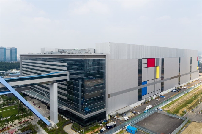
To better address the growing demand for next-generation premium DRAM, Samsung will start the operation of a second semiconductor fabrication line in Pyeongtaek, South Korea, within the second half of this year.

пятница, 21 февраля 2020 г.

Samsung Foundry выиграл большой контракт на производство 5G-чипов для американской Qualcomm


Информационное агентство Reuters в своём эксклюзивном материале сообщило, что контрактное подразделение по выпуску полупроводников Samsung Foundry выиграло контракт на поставку новых чипов Qualcomm.
По информации источников агентства, Samsung будет производить часть чипов из семейства недавно объявленных Q60 для работы с 5G-сетями.
Ожидается, что эти продукты будут выпускаться по технологии 5 нм и, возможно, когда тайвантская TSMC также запустит эти производственные нормы, она также получит заказ от Qualcomm.
Samsung и Qualcomm пока никак не комментируют эту информацию.
Южнокорейский электронный гигант в последние годы активно развивает контрактное полупроводниковое производство и, в частности, выпускает чипы для таких известных корпораций как IBM и Nvidia. В прошлом году Samsung объявил о планах инвестировать до 2030 года $116 миллиардов в развитие полупроводникового производства, не связанного с выпуском чипов памяти.
Очередная сделка с Qualcomm демонстрирует явный прогресс в развитии контактного производства Samsung и получение такого клиента крайне важно для южнокорейцев. Согласно данным TrendForce, в 4-м квартале 2019 году доля Samsung в сегменте контрактного выпуска чипов составила 17,8% против 52,7% у TSMC.
В январе руководство TSMC заявило, что намерено активизировать запуск производства по нормам 5 нм и планирует достичь к концу нынешнего года доли этого техпроцесса на уровне 10%.

Samsung Electronics wins contract to manufacture 5G chips for Qualcomm

Samsung Electronics Co Ltd’s semiconductor manufacturing division has won a contract to make new Qualcomm Inc 5G chips using its most advanced chip-making technology, two sources familiar with the matter said, boosting the Korean firm’s efforts to gain market share against rival Taiwan Semiconductor Manufacturing Co.
Samsung will fabricate at least some of Qualcomm’s X60 modem chips, which will connect devices such as smart phones to 5G wireless data networks. The X60 will be made on Samsung’s 5-nanometer process, the sources said, which makes the chips smaller and more power-efficient than previous generations.
One of the sources said TSMC is also expected to fabricate 5-nanometer modems for Qualcomm. Samsung and Qualcomm declined to comment, and TSMC did not immediately respond to a request for comment.
Best known among consumers for its phones and other electronic devices, Samsung is the world’s second-biggest chip manufacturer through its foundry division, self-supplying many of its own mobile phone parts and also fabricating chips for outside customers such as International Business Machines Corp (IBM) and Nvidia Corp, among others.
But much of Samsung’s semiconductor revenue historically has come from memory chips, whose prices can swing wildly as supply and demand fluctuate. In an attempt to cut its reliance on that volatile market, Samsung announced a plan last year to invest $116 billion in non-memory chips through 2030.
The Qualcomm deal shows progress in winning customers to that effort. Even if Samsung has won only part of the orders, Qualcomm represents a flagship customer for Samsung’s 5-nanometer manufacturing technology. Samsung plans to ramp up that technology this year in an attempt to regain market share against TSMC, which is also starting mass production of 5-nanonmeter chips this year.
The Qualcomm win could boost Samsung’s foundry business because the X60 modem is likely to be used in many mobile devices as they shift to 5G. In the fourth quarter of 2019, Samsung had 17.8% market share versus TSMC’s 52.7%, according to data from TrendForce.
In a separate announcement, Qualcomm said on Tuesday it would begin sending samples of the X60 chips to customers in the first quarter of this year. Qualcomm did not disclose who would manufacture the chips, and Reuters could not learn whether the first batches of chips would be made by Samsung or TSMC.
The Taiwanese company was faster to ramp up high-volume production of chips using the previous 7-nanometer manufacturing process, winning customers such as Apple Inc.
Last month, TSMC executives said they expect to begin ramping up 5-nanometer production in the first half of the year and expect it to make up 10% of the company’s revenue for 2020.
Asked during a January investor conference call how Samsung will compete with TSMC, Shawn Han, senior vice president at Samsung Foundry, said the company planned to expand 5-nanometer mass production by “diversifying customer applications” this year.
Qualcomm designs its own chips but works with outside companies to manufacture them. It has used manufacturing services from both Samsung and TSMC in the past, as well as from China’s Semiconductor Manufacturing International Corp, depending on which foundry’s technology and pricing met its needs for the product at hand.

воскресенье, 26 января 2020 г.

Samsung и TSMC начали гонку за первенство по внедрению 3-нанометрового процесса в полупроводниковой отрасли


Корейский техногигант Samsung Electronics и тайваньская компания TSMC ведут ожесточённую войну на рынке контрактного производства полупроводников, стремясь внедрить новейший 3-нм процесс. Оба производителя хотят начать серийное производство таких продуктов в 2022-м году.
Ожидается, что TSMC, крупнейший в мире контрактный поставщик полупроводников, представит свой 3-нм техпроцесс 29 апреля на технологическом симпозиуме в Северной Америке. TSMC ранее объявила о своей цели массового производства 3-нм полупроводников к 2022 году, но не раскрыла конкретную технологическую дорожную карту. Ожидается, что ради достижения этих целей TSMC начнёт строительство завода на Тайване в этом году.
Ранее Samsung официально объявил, что его инженерам удалось разработать первую в отрасли технологию 3-нм техпроцесса. Ли Джей-ён, вице-президент Samsung Electronics, был проинформирован о технологическом прорыве во время своего визита в Центр исследований полупроводников на заводе в Хвасоне 2 января 2020-го.
Отраслевые эксперты полагают, что Samsung Electronics немного опережает TSMC в сфере внедрения 3-нм техпроцесса. «Мы уже сделали 3-нм образец полупроводника и убедились, что он хорошо работает», - сказал представитель Samsung Electronics. «Мы также предоставили инструменты для проектирования тем компаниям, которые занимаются разработкой полупроводников».
«Производитель микросхем, который первым освоит массовое производство 3-нм продуктов, с большей вероятностью получит заказы на новейшие чипы от компаний, занимающихся разработкой чипов», - говорит Кан Санг-ку, сотрудник  Института стратегических исследований будущего KDB.
Чем более тонкие техпроцессы используются в полупроводниковых микросхемах, тем меньше энергии они потребляют и тем выше их производительность. По сравнению с 5-нм продуктами, 3-нм техпроцесс позволяет уменьшить размеры микросхем и энергопотребление на 35% и 50% соответственно и повысить производительность на 30%.
Samsung Electronics и TSMC также начнут ожесточённую битву в этом году за первенство в освоении массового производства 5-нм чипов. Samsung Electronics завершил разработку 5-нм технологии и планирует начать серийный выпуск продукции в текущем году. TSMC также планирует начать массовое производство 5-нм чипов в 2020-м.
В 4-м квартале 2019 года TSMC заняла 52,7% мирового рынка контрактного производства чипов, а Samsung Electronics - 17,8%.
Напомним, что до недавнего времени Samsung не делал акцента на удовлетворении запросов сторонних заказчиков, используя большую часть полупроводниковой продукции для собственных нужд. Но пару лет назад стратегия в полупроводниковом бизнесе поменялась, и теперь ставка сделана на расширение контрактного производства. Руководством чеболя поставлена цель стать контрактным производителем полупроводниковых продуктов №1 к 2030 году, сообщает портал Business Korea.

Samsung and TSMC Racing to Become First to Start Volume Production of 3-nm Chips

Samsung Electronics of Korea and TSMC of Taiwan are waging a fierce war over a 3-nanometer (nm) foundry process. Both companies are planning to begin volume production of 3-nm products in 2022.
TSMC, the world's No. 1 foundry company, is expected to unveil its 3-nm process technology on April 29 at a technology symposium in North America. TSMC has previously announced its goal to mass-produce 3-nm semiconductors by 2022, but did not disclose a specific technology roadmap. TSMC is expected to begin the construction of a 3-nm plant in Taiwan this year.
In response, Samsung Electronics officially announced earlier this month that it has succeeded in developing the industry’s first 3-nm process technology. Lee Jae-yong, vice chairman of Samsung Electronics, was briefed on the technology breakthrough during his visit to the Semiconductor Research Center at Hwaseong Plant on Jan. 2.
Industry experts believe that Samsung Electronics is slightly ahead of TSMC in 3-nm process development. “We have already made a 3-nm semiconductor sample and verified that it worked nicely,” a Samsung Electronics official said. “We also provided development tools to semiconductor design companies.”
“A chipmaker that starts volume production of 3-nm products first is more likely to win orders for the latest chips from semiconductor design companies,” said Kang Sang-ku, a researcher at the KDB Future Strategic Research Institute
The narrower semiconductor circuit lines are, the less power semiconductors consume and the better they perform. Compared to 5-nm products, 3-nm semiconductors can reduce chip sizes and power consumption by 35 percent and 50 percent, respectively, and increase performance by 30 percent.
Samsung Electronics and TSMC will also stage a fierce battle this year to become the first to start volume production of 5-nm chips. Samsung Electronics has completed the development of a 5-nm process and is planning to begin volume production of 5-nm products from this year. TSMC is also aiming to start mass production of 5-nm products this year.
In the fourth quarter of 2019, TSMC recorded a 52.7 percent share of the global foundry market, while Samsung Electronics accounted for 17.8 percent. Samsung Electronics has set the goal of becoming the No. 1 system semiconductor maker by 2030.

воскресенье, 5 января 2020 г.

Samsung инвестирует $116 миллиардов в контрактное производство чипов


Samsung Electronics активно инвестирует в бизнес в области услуг контрактного производства чипов, чтобы конкурировать с тайваньской TSMC, сообщает информационное агентство Bloomberg.
В ближайшие 10 лет Samsung намерен инвестировать порядка 116 миллиардов долларов на контрактное производство полупроводниковой продукции. $64 миллиарда будут потрачены на исследования и разработки (R&D), а оставшиеся $69 миллиардов пойдут на расширение производственных мощностей, что позволит создать 15.000 рабочих мест.
Одно из направлений для инвестиций - процесс экстремальной ультрафиолетовой литографии (EUV, Extreme Ultraviolet Lithography). Его использование должно помочь южнокорейскому гиганту освоить 5-нм, 3-нм и более тонкие технологические процессы.
По оценкам TrendForce, в октябре-декабре 2019 года оборот контрактного подразделения Samsung Foundry вырос на 19,3% в годовом исчислении и достигнет 3,47 миллиарда долларов США.
Несмотря на впечатляющий рост, Samsung пока ещё значительно уступает TSMC. В 4-м квартале 2019 года выручка TSMC достигла 10,25 миллиарда долларов, что на 8,6% выше прошлогоднего результата. Тройку лидеров рынка фаундри-услуг традиционно замкнет GlobalFoundries с выручкой в 1,56 миллиарда долларов (+0,1%).

Samsung invests $ 116 billion in contract manufacturing chips

Bloomberg, 22/12/2019

Technology giants are increasingly designing their own semiconductors to optimize everything from artificial intelligence tasks to server performance and mobile battery life. Google has the Tensor Processing Unit, Apple Inc. has the A13 Bionic and Amazon.com Inc. has the Graviton2. What the titans all lack, however, is a factory to build the new chips they are dreaming up.
Enter Samsung Electronics Co., which is planning a decade-long, $116 billion push for their business. The South Korean company is investing heavily in the next step in miniaturizing semiconductors, a process called extreme ultraviolet lithography (EUV). It’s by far the priciest manufacturing upgrade Samsung has ever attempted, a risky bid to move beyond its established business of cranking out commoditized silicon and to leapfrog the incumbent leaders in the $250 billion foundry and logic-chip industry.
“A new market is opening up,” Yoon Jong Shik, executive vice president of Samsung’s foundry business, said at a forum recently held in Seoul. “Companies like Amazon, Google and Alibaba, which lack experience in silicon design, are seeking to make chips with their own concept ideas in order to boost their services. I think this would bring a significant breakthrough for our non-memory chip business.”
Samsung is a relative underdog in this growing field. The foundry business - as the manufacturing of chips for companies like Google and Qualcomm Inc. is known - is dominated by Taiwan Semiconductor Manufacturing Co. with more than half the market, according to TrendForce Corp. data that puts Samsung at 18%.
TSMC also took over Apple’s A-series processor manufacturing from Samsung, which was the original production partner. Samsung plans to spend about $10 billion per year on equipment, research and development over the next decade, but TSMC is even more ambitious with capital expenditure of around $14 billion for this year and next.
“It is not just a matter of willingness,” said CW Chung, head of pan-Asia technology at Nomura Financial Investment Co., in assessing Samsung’s chances of success. “Chip-making is like a composite art. Unless there are enough supports for all-round social infrastructures, it’d be a scarcely achievable goal.”
To win over clients, top Samsung executives are touring major cities from San Jose to Munich to Shanghai, hosting foundry forums and negotiating deals. ES Jung, president and general manager for the foundry business, is the frontman delivering Samsung’s “can-do” spiel at every gathering, where his practiced joke is to suggest that his initials stand for “engineering sample.”
“The complexity of the lines drawn by the EUV equipment is similar to building a spaceship,” said Jung while unveiling a $17 billion EUV plant in Hwaseong earlier this year, flanked by Samsung heir and de-facto boss Jay Y. Lee and South Korean President Moon Jae-in. The fab is planned to start mass production in February 2020.
A single EUV machine from ASML Holding NV costs $172 million and Samsung is setting up dozens of them in Hwaseong in an effort to be first with the technology. TSMC and Samsung are both expected to reach 5-nanometer production processes with EUV in the new year, which means they’ll have only each other to compete with in a market that’s only set to expand. And once they ramp up and achieve economies of scale, the overall process cycle time is likely to decrease by 20% and the foundry capacity output will increase by 25%, according to a Citigroup Inc. research report.
“TSMC is too busy with orders pouring in for new products as we enter into the 5G era,” said Greg Roh, senior vice president at Hyundai Motor Securities. “For Samsung, that’s bringing a good chance to expand their market share by offering lower prices and delivery schedules to meet clients’ needs.”
Samsung is collaborating with major clients on designing and manufacturing custom chips and that work is already starting to add to its revenue, according to one Samsung executive who has direct knowledge of the matter. The push toward bespoke processors in Silicon Valley and China is opening up fresh opportunities and Samsung already has established relationships, as demonstrated by its recent announcement that it’ll produce an AI chip for Baidu Inc. early next year.
Officials at Samsung believe the company has a competitive edge from its experience building both the chips and the devices that they go into. It is thus able to foresee and address the engineering requirements of its clients. Samsung believes its other trump card is an ability to package memory and logic chips into a single module, improving power and space efficiency. Analysts do warn, however, that some companies are wary about outsourcing production to a direct competitor in the consumer electronics market - lest Samsung learns and copies their chip designs in its own products.
“Ultimately, the success of Samsung’s logic chip business depends on its market positioning,” Hsu said. “On the foundry side, Samsung needs to eliminate its clients’ suspicions of Samsung LSI being a potential competitor.”
Samsung is reaching out to smartphone-making rivals and has already agreed to sell 5G Exynos chips to Vivo. At the same time, it’s going to be manufacturing Qualcomm’s 5G mobile chipset using the same EUV process. On yet another front, the company is competing with foundry customer Sony Corp. in the growing market for image sensors, having this year unveiled an unprecedented 108-megapixel camera for smartphones. “I think Samsung’s CMOS image sensor business will continue to do well, riding on the industry boom,” said Bloomberg Intelligence analyst Anthea Lai.
If Samsung can move ahead technologically, it should find no shortage of customers for its varied semiconductor offerings. Though China is increasingly turning to domestic suppliers for all things tech, the greater efficiency of EUV chips may be key in helping Samsung solicit business from the world’s second-biggest economy.
“The increased demand for in-house chips spells good news for the growth of the foundry industry,” TrendForce analyst Chris Hsu said.

воскресенье, 22 декабря 2019 г.

Контрактный производитель чипов Samsung Foundry объявил о совместной разработке с китайской Baidu в области искусственного интеллекта


Построенный на базе 14-нм техпроцесса и технологии упаковки I-CubeTM от Samsung, процессор Baidu KUNLUN призван расширить экосистему искусственного интеллекта и трансформировать пользовательский опыт

Компания Baidu, Inc., крупнейшая китайская поисковая система, и Samsung Electronics, мировой лидер в области передовых полупроводниковых технологий, объявляют о создании первого ускорителя искусственного интеллекта – процессора Baidu KUNLUN, который предназначен для работы в самых различных платформах, от облака до периферии. Партнёры готовы запустить его в массовое производство уже в начале следующего года.
В основе чипа Baidu KUNLUN лежит передовая разработка Baidu XPU – собственная архитектура нейронных процессоров для облачных и граничных вычислений, в нём используется 14-нм техпроцесс и технология пакетирования I-Cube™ от Samsung.
Новый процессор обеспечивает пропускную способность памяти на уровне 512 гигабайт в секунду (Гб/с) и позволяет осуществлять до 260 тераопераций в секунду (TOPS) при энергопотреблении 150Вт. Кроме того, в чипе поддерживается Ernie, предварительно обученная нейронная модель для обработки данных на естественном языке, которая осуществляет построение логических выводов втрое быстрее, чем традиционная модель ускорения GPU / FPGA.
Благодаря большой вычислительной мощности и низкому энергопотреблению новый процессор позволит Baidu с высокой эффективностью выполнять самые различные задачи, в том числе запускать масштабные рабочие нагрузки с использованием искусственного интеллекта, например, ранжировать поисковые результаты, распознавать речь, изображения и естественные языки, а также разрабатывать системы автономного вождения и реализовывать платформы глубокого обучения, такие как PaddlePaddle.
В рамках пилотного сотрудничества Baidu предоставит свои передовые платформы искусственного интеллекта для обеспечения максимальной производительности, а Samsung запустит производство на своих полупроводниковых фабриках процессоров для высокопроизводительных вычислений (HPC), предназначенных для работы в облаке и на периферии.
«Мы рады оказаться в числе лидеров индустрии высокопроизводительных вычислений вместе с Samsung Foundry, – говорит Оуянг Цзянь (OuYang Jian), ведущий специалист по архитекторе полупроводников в Baidu. – Baidu KUNLUN – это чрезвычайно сложный проект. Он не только обеспечивает высокий уровень надёжности и производительности, но и задействует самые передовые технологии в полупроводниковой отрасли. Благодаря инновационным технологическим процессам Samsung и высоким компетенциям специалистов, работающих на полупроводниковых фабриках корпорации, мы смогли достичь нашей цели и даже превзойти её, предложив более качественный пользовательский опыт при работе с искусственным интеллектом».
«Проект Baidu KUNLUN представляет собой важную веху для Samsung Foundry, поскольку теперь мы расширяем сферу нашей деятельности и производим не только микросхемы для мобильных устройств, но и процессоры для центров обработки данных, разрабатывая и запуская в массовое производство чипы для ускорения задач искусственного интеллекта. Samsung предоставит комплексные решения для всего цикла полупроводникового производства, начиная с оказания помощи в проектировании чипов и заканчивая передовыми техпроцессами, такими как 5LPE, 4LPE, а также технологией 2,5D упаковки», – говорит Райан Ли (Ryan Lee), вице-президент по маркетингу полупроводниковых решений Samsung Electronics.
Поскольку в различных приложениях, таких как рабочие нагрузки искусственного интеллекта или HPC-вычисления, постоянно требуется более высокая производительность, особую актуальность сегодня приобретают технологии пакетирования (chip integration technology). Представленная Samsung технология интеграции I-Cube™, соединяющая логический чип и память с высокой пропускной способностью (HBM2) с подложкой (interposer), позволяет добиться ещё более высокой плотности и пропускной способности при минимальном размере за счёт использования дифференцированных решений Samsung.
По сравнению с предыдущими разработками новые решения позволяют значительно увеличить производительность процессора и обеспечивают прирост вычислительной мощности / целостности сигнала более чем на 50%. Считается, что внедрение I-CubeTM ознаменует начало новой эпохи на рынке гетерогенных вычислений. Кроме того, Samsung разрабатывает более совершенные технологии пакетирования, такие как технологию RDL-подложки (redistribution layers), а также интегрированные корпуса с 4x и 8x HBM памяти.

Baidu and Samsung Electronics Ready for Production of Leading-Edge AI Chip for Early Next Year

Designed based on Samsung’s 14nm process and I-Cube TM package technology, 
Baidu KUNLUN chip to expand AI ecosystem and transform the user experience

Baidu, a leading Chinese-language Internet search provider, and Samsung Electronics, a world leader in advanced semiconductor technology, today announced that Baidu’s first cloud-to-edge AI accelerator, Baidu KUNLUN, has completed its development and will be mass-produced early next year.
Baidu KUNLUN chip is built on the company’s advanced XPU, a home-grown neural processor architecture for cloud, edge, and AI, as well as Samsung’s 14-nanometer (nm) process technology with its I-Cube™ (Interposer-Cube) package solution.
The chip offers 512 gigabytes per second (GBps) memory bandwidth and supplies up to 260 Tera operations per second (TOPS) at 150 watts. In addition, the new chip allows Ernie, a pre-training model for natural language processing, to infer three times faster than the conventional GPU/FPGA-accelerating model.
Leveraging the chip’s limit-pushing computing power and power efficiency, Baidu can effectively support a wide variety of functions including large-scale AI workloads, such as search ranking, speech recognition, image processing, natural language processing, autonomous driving, and deep learning platforms like PaddlePaddle.
Through the first foundry cooperation between the two companies, Baidu will provide advanced AI platforms for maximizing AI performance, and Samsung will expand its foundry business into high performance computing (HPC) chips that are designed for cloud and edge computing.
“We are excited to lead the HPC industry together with Samsung Foundry,” said OuYang Jian, Distinguished Architect of Baidu. “Baidu KUNLUN is a very challenging project since it requires not only a high level of reliability and performance at the same time, but is also a compilation of the most advanced technologies in the semiconductor industry. Thanks to Samsung’s state of the art process technologies and competent foundry services, we were able to meet and surpass our goal to offer superior AI user experience. ”
“We are excited to start a new foundry service for Baidu using our 14nm process technology,” said Ryan Lee, vice president of Foundry Marketing at Samsung Electronics. “Baidu KUNLUN is an important milestone for Samsung Foundry as we’re expanding our business area beyond mobile to datacenter applications by developing and mass-producing AI chips. Samsung will provide comprehensive foundry solutions from design support to cutting-edge manufacturing technologies, such as 5LPE, 4LPE, as well as 2.5D packaging.”
As higher performance is required in diverse applications such as AI and HPC, chip integration technology is becoming more and more important. Samsung’s I-Cube™ technology, which connects a logic chip and high bandwidth memory (HBM) 2 with an interposer, provides higher density/ bandwidth on minimum size by utilizing Samsung’s differentiated solutions.
Compared to previous technology, these solutions maximize product performance with more than 50% improved power/signal integrity. It is anticipated that I-Cube™ technology will mark a new epoch in the heterogeneous computing market. Samsung is also developing more advanced packaging technologies, such as redistribution layers (RDL) interposer and 4x, 8x HBM integrated package.

суббота, 30 ноября 2019 г.

Intel обратилась к Samsung за помощью в производстве процессоров


Южнокорейское информагентство Yonhap сообщило, что корпорация Samsung Electronics согласилась начать выпуск центральных процессоров для Intel. Неделю назад в Intel намекнули на возможность подобного развития событий. В открытом письме, в котором компания призналась в своей неспособности преодолеть дефицит процессоров, Intel сообщила, что намерена попросить помощи у стороннего производителя. Поскольку Intel давно работает с тайваньской TSMC, все решили, что заказ будет выполнять именно она. Однако выяснилось, что помощь американцам готовы оказать в Samsung.
Если Samsung действительно начнёт выпускать для Intel центральные процессоры, то это станет важным прецедентом. Поначалу это будут 14-нм продукты, но если сотрудничество окажется успешным, Samsung может заинтересовать Intel как производитель 7-нм продукции. Для Intel это возможность быстро развернуть поставки 7-нм процессоров, хотя американской компании приходится думать о долгосрочной перспективе по загрузке и поддержке собственных предприятий.
Для Samsung сотрудничество с Intel как крупного заказчика ― это шанс укрепить контрактное производство. Главная опасность для Samsung кроется в производственных мощностях TSMC, которая работает с множеством сторонних партнёров.
В последнее время Samsung расширяет собственное контрактное производство и для этого вкладывает в новейшие техпроцессы и поточные линии огромные деньги. Новый долгосрочный план Samsung по развитию полупроводникового производства (в том числе контрактного) предусматривает инвестиции в этот сектор $112,9 миллиарда. Это гигантская сумма, которая позволит планомерно отбирать заказы у TSMC и укреплять рыночную долю южнокорейского гиганта.
Комментируя возможное сотрудничество Samsung и Intel, агентство Yonhap ссылается на свои осведомлённые источники. И хотя детали предполагаемой сделки ещё неизвестны, отраслевые наблюдатели говорят, что для каждой из компаний это может быть важной вехой в развитии бизнеса.

Samsung to supply PC CPUs to Intel: sources

Samsung Electronics has agreed to supply central processing units for computers to Intel to help address the US chipmaker’s supply issues, industry sources said Nov. 28. 
Intel has been struggling to meet demand for 14-nanometer chips for PCs since late 2018 and recently issued an apology to its customers for shipment delays.
According to semiconductor industry sources, Intel has chosen Samsung to be its third-party foundry to ramp up its 14-nm production capacity as part of efforts to deal with its prolonged processor shortage.
“Samsung was chosen as a partner as it is one of a couple of foundries that can meet Intel’s demand for 14-nm production, among other reasons,” the source said, without elaborating on the production schedule. 
Intel is a global leader in CPUs, which power desktops, servers and embedded devices, and is followed by Advanced Micro Devices. 
The latest agreement is expected to boost Samsung‘s bid to bolster its non-memory chip business after announcing a semiconductor investment plan worth 133 trillion won ($112.9 billion) earlier this year.

пятница, 11 октября 2019 г.

Представлены новые микросхемы для автономных машин с ДВС и электромобилей на мероприятии Samsung Foundry Forum 2019 в Мюнхене


Для удовлетворения растущего спроса на рынках автономных авто и электромобилей Европы, Ближнего Востока и Африки Samsung предлагает чипы на основе техпроцессов 28 нм FDS и 14 нм

Samsung Electronics, мировой лидер в области передовых полупроводниковых технологий, представил расширенное портфолио инновационных микросхем для автомобильной промышленности Европы, Ближнего Востока и Африки.
Поскольку полупроводники в этом регионе востребованы в широком спектре отраслей, включая автомобилестроение, потребительскую электронику, сетевые технологии и Интернет вещей (IoT), Samsung представил ряд специализированных технологий, таких как FD-SOI, радиочастота (RF) и встроенная память, а также полный набор узлов процесса. Для повышения доступности полупроводниковых решений транснациональный гигант продемонстрировал инновационные платформы, которые объединяют ключевые технические элементы для развёртывания решений на базе 5G, IoT, высокопроизводительных вычислений (HPC) для создания «умных» автомобилей.
«В связи с активным развитием европейской автомобильной промышленности, рынок полупроводниковых решений для этой отрасли привлекает значительное внимание и, как ожидается, будет стремительно развиваться, чтобы удовлетворить растущий спрос в области автономных ДВС-машин и электромобилей», – отметил д-р И Эс Джанг (ES Jung), президент и глава направления производства полупроводников в Samsung Electronics.
Сейчас Samsung производит несколько полупроводниковых продуктов для автопрома, таких как помощник по вождению и информационно-развлекательные системы, в основном на базе 28-нанометровых (нм) FD-SOI и 14-нм техпроцессов. Для того, чтобы удовлетворить растущие запросы клиентов, Samsung планирует в ближайшем будущем представить решения на базе техпроцессов до 8 нм.
Samsung также уделяет особое внимание функциональной безопасности и надёжности компонентов, что имеет решающее значение в автомобильной промышленности, поскольку любой сбой может привести к аварии, травме или другим серьёзным последствиям. производитель уже доказал свою способность разрабатывать решения, соответствующие стандартам автомобильной индустрии, и получил сертификат ISO 26262 компании TÜV Rheinland, а также требованиям надёжности AEC-Q100 и системы управления качеством IATF 16969.

Samsung Introduces Advanced Automotive Foundry Solutions Tailored to EMEA Market at Samsung Foundry Forum 2019 Munich

To address the growing demand in the autonomous and electric vehicle market, Samsung offers various foundry solutions based on 28nm FDS and 14nm process

Samsung Electronics, a world leader in advanced semiconductor technology, today unveiled an expanded portfolio of cutting-edge foundry solutions at its Samsung Foundry Forum (SFF) 2019 Munich.
Samsung attracted more than 200 industry experts from fabless companies and foundry partners, and 16 partner booths displayed advanced foundry technology trends, a significant increase in both numbers compared to last year, representing a more solid customer base of Samsung Foundry as well as greater collaboration in Europe, Middle East, and Africa (EMEA).
Since the EMEA semiconductor market is in demand across a wide range of applications including automotive, consumer, network, and internet-of things (IoT), Samsung introduced various specialty technologies, such as FD-SOI, radio frequency (RF), and embedded memory along with comprehensive portfolio of foundry process nodes.
Samsung Electronics showcased its state-of-the-art foundry platforms that bring together essential technical elements for new-age applications, including 5G, IoT, automotive, and high performance computing (HPC), while expanding its design solution partners to improve global customers’ access to Samsung’s foundry solutions.
“It is a great honor to host our global foundry forum with increasing number of attendees every year. The forum has helped us work closely with our customers and strengthen Samsung’s foundry ecosystem,” said Dr. ES Jung, president and head of foundry business at Samsung Electronics, in the keynote speech. “We will strive to get more customer trust and be the best partner possible to prepare for the future with.”
Given the robustness of the European automotive industry, the foundry platform for automotive semiconductor market is drawing considerable attention, and is expected to rapidly grow to address the increasing demand in the autonomous and electric vehicle market.
Samsung is currently producing several automotive semiconductor products such as driving assistant and infotainment systems, mainly based on its 28-nanometer (nm) FD-SOI and 14nm process nodes. In order to respond to increasing customer inquiries, Samsung plans to expand its automotive process nodes to 8nm in near future.
Samsung is also focusing on functional safety and component reliability, which are critically important in the automotive industry, since any failure could cause serious consequences of accident or injury.
Samsung has already proven its ability to design IPs to meet the required automotive standard, and received the ISO 26262 certification for functional safety in automotive components from TÜV Rheinland. Complying with reliability standard AEC-Q100 and IATF 16969 quality management system, it is also preparing for automotive semiconductor production.
Meanwhile, in cooperation with ecosystem partners, Samsung will host its first SAFE™ (Samsung Advanced Foundry Ecosystem) Forum on Oct 17 in San Jose, to introduce Samsung’s IP, Electronic Design Automation (EDA), and packaging solutions in detail for foundry partners.

среда, 15 мая 2019 г.

Samsung огласил планы развития своего полупроводникового бизнеса


В сегодняшнем официальном пресс-релизе Samsung Electronics сообщает о своих планах по развитию технологических процессов в полупроводниковом бизнесе. Программа озвучена в ходе мероприятия Samsung Foundry Forum 2019, проходящем в Санта-Кларе (штат Калифорния, США).
Актуальным достижением лидер электронной индустрии считает создание цифровых проектов опытных 3-нм чипов на основе патентованных транзисторов MBCFET. Это транзисторы с множеством горизонтальных наностраничных каналов в вертикальных FET-затворах (Multi-Bridge-Channel FET).
В содружестве с американской IBM Samsung разрабатывал несколько иную технологию производства транзисторов с каналами, полностью окружёнными затворами (GAA или Gate-All-Around). Каналы предполагалось делать тонкими в виде нанопроводов. Впоследствии Samsung отошёл от этой схемы и запатентовал структуру транзисторов с каналами в виде наностраниц. Такая структура позволяет управлять характеристиками транзисторов за счёт манипуляции как числом страниц (каналов), так и регулируя ширину страниц. Для классической технологии FET подобный манёвр невозможен. Чтобы увеличить мощность FinFET-транзистора необходимо умножать число FET-рёбер на подложке, а это расход площади. Характеристики транзистора MBCFET можно менять в рамках одного физического затвора, для чего нужно задать ширину каналов и их количество.
Наличие цифрового проекта (taped out) опытного чипа для выпуска с использованием техпроцесса GAA позволило Samsung определить границы возможностей транзисторов MBCFET.
Следует учитывать, что пока это данные компьютерного моделирования и окончательно о новом техпроцессе можно будет судить только после запуска его в массовое производство. Тем не менее, точка отсчёта уже имеется. В корпорации сообщили, что переход от 7-нм техпроцесса (очевидно, первого поколения) на техпроцесс GAA обеспечит сокращение площади кристалла на 45% и снижение потребления на 50%. Если не экономить на потреблении, то производительность можно увеличить на 35%. Ранее Samsung экономию и рост производительности при переходе на 3-нм техпроцесс перечислял через запятую. Оказалось всё-таки, или одно, или другое.
Важным моментом для популяризации 3-нм техпроцесса производитель считает подготовку общедоступной облачной платформы для независимых разработчиков чипов и бесфабричных компаний. В Samsung не стали прятать среду разработки, проверки проектов и библиотеки на производственных серверах. Для проектировщиков во всём мире будет доступна платформа SAFE (Samsung Advanced Foundry Ecosystem Cloud). Облачная платформа SAFE создавалась с участием таких крупнейших публичных облачных сервисов, как Amazon Web Services (AWS) и Microsoft Azure. Свои инструменты для проектирования в рамках SAFE предоставили разработчики систем проектирования компаний Cadence и Synopsys. Это обещает упростить и удешевить процесс создания новых решений для техпроцессов Samsung.
Возвращаясь к 3-нм техпроцессу Samsung, добавим, вендор представил первую версию пакета для разработки чипов ― 3nm GAE PDK Version 0.1. С его помощью уже сегодня можно приступить к проектированию 3-нм решений или, по крайней мере, подготовиться к встрече этого техпроцесса Samsung, когда он станет массовым.
Дальнейшие планы Samsung обстоят следующим образом. Во второй половине текущего года будет запущено массовое производство чипов с использованием 6-нм техпроцесса. Тогда же завершится разработка 4-нм техпроцесса. Разработка первых продуктов Samsung с использованием 5-нм техпроцесса будет завершена нынешней осенью, с запуском в производство в первой половине следующего года. Также до конца текущего года Samsung завершит разработку техпроцесса 18FDS (18 нм на пластинах FD-SOI) и 1-Гбит чипов eMRAM. Техпроцессы от 7 нм до 3 нм будут использовать сканеры EUV с нарастающей интенсивностью, и при этом на счету будет каждый нанометр. Дальше за путь вниз каждый шаг будет даваться с боем.

Samsung Electronics’ Leadership in Advanced Foundry Technology Showcased with Latest Silicon Innovations and Ecosystem Platform

New 3GAE PDK enables customers’ early design work to enhance design competitiveness
SAFE™-Cloud platform provides reliable turnkey design environment to accelerate design workflow for fabless companies and design houses

Samsung Electronics, a world leader in advanced semiconductor technology, today announced its ongoing commitment to foundry innovation and service at the Samsung Foundry Forum 2019 USA, providing the silicon community with wide-ranging updates on technology advances that support the most demanding applications of today and tomorrow.
The event, held today in Santa Clara, California, features top Samsung executives and industry experts reviewing progress on semiconductor technologies and foundry platform solutions that enable developments in artificial intelligence (AI), machine learning, 5G networking, automotive, the Internet of Things (IoT), advanced data centers and many other domains.
“We stand at the verge of the Fourth Industrial Revolution, a new era of high-performance computing and connectivity that will advance the daily lives of everyone on the planet,” said Dr. ES Jung, President and head of Foundry Business at Samsung Electronics.
“Samsung Electronics fully understands that achieving powerful and reliable silicon solutions requires not only the most advanced manufacturing and packaging processes as well as design solutions, but also collaborative foundry-customer relationships grounded on trust and shared vision. This year’s Foundry Forum is filled with compelling evidence of our commitment to progress in all those areas, and we’re honored to host and converse with our industry’s best and brightest,” Dr. Jung added.

Highlights from the U.S. Foundry Forum include:

The New 3nm GAE PDK Version 0.1 is Ready

Samsung’s 3nm Gate-All-Around (GAA) process, 3GAE, development is on track. The company noted today that its Process Design Kit (PDK) version 0.1 for 3GAE has been released in April to help customers get an early start on the design work and enable improved design competitiveness along with reduced turnaround time (TAT).
Compared to 7nm technology, Samsung’s 3GAE process is designed to provide up to a 45 percent reduction in chip area with 50 percent lower power consumption or 35 percent higher performance. The GAA-based process node is expected to be widely adopted in next-generation applications, such as mobile, network, automotive, Artificial Intelligence (AI) and IoT.
Conventional GAA based on nanowire requires a larger number of stacks due to its small effective channel width. On the other hand, Samsung’s patented version of GAA, MBCFET™ (Multi-Bridge-Channel FET), uses a nanosheet architecture, enabling greater current per stack.
While FinFET structures must modulate the number of fins in a discrete way, MBCFET™ provides greater design flexibility by controlling the nanosheet width. In addition, MBCFET™’s compatibility with FinFET processes means the two can share the same manufacturing technology and equipment, which accelerates process development and production ramp-up.
Samsung recently taped out the 3GAE test vehicle design and will focus on improving its performance and power efficiency going forward.

The Launching of a New SAFE™–Cloud Program

As part of its ongoing efforts to support and enhance customers’ entire design workflow, Samsung Electronics launched the Samsung Advanced Foundry Ecosystem Cloud (SAFE™-Cloud) program. It will provide customers with a more flexible design environment through collaboration with major public cloud service providers, such as Amazon Web Services (AWS) and Microsoft Azure, as well as leading Electronic Design Automation (EDA) companies, including Cadence and Synopsys.
To date, most foundry customers have built and managed design infrastructure on their own servers. The SAFE™-Cloud program reduces this burden and supports easier, faster and more efficient design efforts by providing an excellent turnkey design environment with extensive process information (PDK, design methodologies), EDA tools, design assets (IP, library) and design services.
Customers can be assured of as much server and storage space as they need, as well as a safe environment optimized for chip design, due to Samsung Electronics’ verification of SAFE™-Cloud’s security, applicability and expandability.
Utilizing the SAFE™-Cloud platform, Samsung was able to accelerate the development of its 7nm and 5nm cell libraries in collaboration with Synopsys. In addition, Samsung, Gaonchips – a fabless design company in Korea – and Cadence have successfully completed design verification based on the platform.
“Making up-front investments in high-performance computing (HPC) servers and systems can be a challenge for a company like us,” said Kyu Dong Jung, CEO of Gaonchips. “SAFE™-Cloud offers us a very flexible design environment without requiring investment in additional infrastructure, as well as reduced design TAT. I expect this program to provide more tangible business and technical benefits to us and the entire fabless industry.”

Process Technology Roadmap and Advanced Packaging Updates

Samsung’s roadmap includes four FinFET-based processes from 7nm down to 4nm that leverage extreme ultraviolet (EUV) technology as well as 3nm GAA, or MBCFET™.
In the second half of this year, Samsung is scheduled to start the mass production of 6nm process devices and complete the development of 4nm process.
The product design of Samsung’s 5nm FinFET process, which was developed in April, is expected to be completed in the second half of this year and go under mass production in the first half of 2020.
Extensions of the company’s FD-SOI (FDS) process and eMRAM together with an expanded set of state-of-the-art package solutions were also unveiled at this year’s Foundry Forum. Development of the successor to the 28FDS process, 18FDS, and eMRAM with 1Gb capacity will be finished this year.

среда, 17 апреля 2019 г.

Samsung объявляет о завершении разработки технологии изготовления чипов по 5-нм техпроцессу, заметно опередив конкурентов


Samsung активно использует своё преимущество как первопроходца полупроводниковой литографии с применением сканеров EUV-диапазона. Пока конкуренты из TSMC только готовится начать использовать сканеры с длиной волны 13,5нм, адаптировав их для выпуска чипов в рамках второго поколения техпроцесса с нормами 7 нм, Samsung идёт дальше и заявляет о завершении разработки техпроцесса с проектными нормами 5нм. Более того, южнокорейский техногигант объявил о начале приёма заказов на выпуск 5-нм решений для производства на мультипроектных пластинах. Это означает, что Samsung готов принимать цифровые проекты чипов с указанными нормами и выпускать опытные партии рабочего 5-нм кремния.
Быстро перейти от предложения 7-нм техпроцесса с EUV на производство 5-нм решений (также с EUV) мэйджору отрасли помогло то обстоятельство, что Samsung сохранил совместимость проектных элементов (IP), инструментов проектирования и контроля. Кроме прочего это означает, что клиенты сэкономят средства на приобретение средств проектирования, тестирования и готовых IP-блоков. Наборы PDK для проектирования, методология (DM, design methodologies) и платформы автоматического проектирования EDA стали доступны ещё в рамках разработки чипов для 7-нм норм Samsung с EUV в 4-м квартале прошлого года. Все эти инструменты обеспечат разработку цифровых проектов также для техпроцесса 5нм с транзисторами FinFET.
По сравнению с 7-нм EUV-техпроцессом, который вендор запустил в октябре прошлого года, 5-нм техпроцесс обеспечит увеличение эффективности использования площади кристалла на 25% (при этом Samsung пока избегает прямых заявлений о снижении размеров площади кристалл на 25%, что оставляет ему пространство для манёвра). Также переход на 5-нм техпроцесс позволит либо снизить на 20% энергопотребление чипов, либо повысить на 10% производительность решений. Ещё одним бонусом станет сокращение числа фотомасок, которые необходимы для производства полупроводников.
Выпуском продукции с использованием сканеров EUV займётся предприятие Samsung Fab S3, которое расположено в городе Хвасон. Во 2-й половине текущего года вендор завершит строительство нового корпуса рядом с Fab S3, которое будет готово выпускать чипы с использованием EUV-техпроцессов в следующем году, говорится в официальном пресс-релизе южнокорейского техногиганта.

Samsung Successfully Completes 5nm EUV Development to Allow Greater Area Scaling and Ultra-low Power Benefits

Samsung Electronics makes major strides in EUV-based advanced nodes, including 7nm mass production and 6nm customer tape-out

Samsung Electronics, a world leader in advanced semiconductor technology, today announced that its 5-nanometer (nm) FinFET process technology is complete in its development and now is ready for customers’ samples. By adding another cutting-edge node to its extreme ultraviolet (EUV)-based process offerings, Samsung is proving once again its leadership in the advanced foundry market.
Compared to 7nm, Samsung’s 5nm FinFET process technology provides up to a 25 percent increase in logic area efficiency with 20 percent lower power consumption or 10 percent higher performance as a result of process improvement to enable us to have more innovative standard cell architecture.
In addition to power performance area (PPA) improvements from 7nm to 5nm, customers can fully leverage Samsung’s highly sophisticated EUV technology. Like its predecessor, 5nm uses EUV lithography in metal layer patterning and reduces mask layers while providing better fidelity.
Another key benefit of 5nm is that we can reuse all the 7nm intellectual property (IP) to 5nm. Thereby 7nm customers’ transitioning to 5nm will greatly benefit from reduced migration costs, pre-verified design ecosystem, and consequently shorten their 5nm product development.
As a result of the close collaboration between Samsung Foundry and its ‘Samsung Advanced Foundry Ecosystem (SAFE™)’ partners, a robust design infrastructure for Samsung’s 5nm, including the process design kit (PDK), design methodologies (DM), electronic design automation (EDA) tools, and IP, has been provided since the fourth quarter of 2018. Besides, Samsung Foundry has already started offering 5nm Multi Project Wafer (MPW) service to customers.
“In successful completion of our 5nm development, we’ve proven our capabilities in EUV-based nodes,” said Charlie Bae, Executive Vice President of Foundry Business at Samsung Electronics. “In response to customers’ surging demand for advanced process technologies to differentiate their next-generation products, we continue our commitment to accelerating the volume production of EUV-based technologies.”
In October 2018, Samsung announced the readiness and its initial production of 7nm process, its first process node with EUV lithography technology. The company has provided commercial samples of the industry’s first EUV-based new products and has started mass production of 7nm process early this year.
Also, Samsung is collaborating with customers on 6nm, a customized EUV-based process node, and has already received the product tape-out of its first 6nm chip.
Mr. Bae continued, “Considering the various benefits including PPA and IP, Samsung’s EUV-based advanced nodes are expected to be in high demand for new and innovative applications such as 5G, artificial intelligence (AI), high performance computing (HPC), and automotive. Leveraging our robust technology competitiveness including our leadership in EUV lithography, Samsung will continue to deliver the most advanced technologies and solutions to customers.”
Samsung foundry’s EUV-based process technologies are currently being manufactured at the S3-line in Hwaseong, Korea. Additionally, Samsung will expand its EUV capacity to a new EUV line in Hwaseong, which is expected to be completed within the second half of 2019 and start production ramp-up from next year.

5nm: A Catalyst of the Fourth Industrial Revolution and What It Means for Semiconductor Innovations

by Daewon Ha
Logic TD team, Semiconductor R&D Center, Samsung Electronics

This week, Samsung Electronics announced that its 5-nanometer(nm) FinFET process technology based on EUV lithography  is now ready for production. This is a remarkable accomplishment and testament to the capability of our colleagues at the S3 wafer fab in Hwaseong, Korea and their supply chain partners.
For me, what is most exciting about this milestone is that it highlights how far the semiconductor industry innovations have come today and provides a glimpse into the evolutions that will shape the industry of tomorrow.
Consider that the 5nm process is here in just six months after last October’s unveiling of the first commercial application of EUV in our 7nm process. It’s a rapid progress made possible in large part by running thousands of wafer layers through EUV exposure systems each week. Hands-on experience is the only way to ascend the EUV learning curve, and that body of knowledge is growing daily.
In the learning process, we’re seeing one of the biggest and broadest benefits of EUV – the simplification of design by moving away from increasingly complex multi-patterning lithography strategies. While still early, it’s increasingly clear that the reduced number of mask steps and more straightforward process is nothing short of a revolution for silicon designers. Sighs of relief will be heard as EUV will be seamlessly incorporated into the existing design architectures.
Samsung’s 5nm is the next step in the evolution of EUV. 5nm will be more efficient and feature new innovations including Samsung’s proprietary Smart Diffusion Break (SDB) transistor architecture. One of the most important aspects of 5nm is that it supports 25 percent area reduction and 10 percent performance improvement or 20 percent power reduction than 7nm.
Also, it will be largely design-rule compatible with the existing design of 7nm. Therefore, it is essentially a recharacterization of the technology, not redesign, which will substantially reduce time and the cost of implementation. This combination of technological advance and economic advantage is very much in line with a grand tradition of the semiconductor industry.
This merging of technological advancement and economic benefits is very much in line with the grand tradition in the semiconductor industry as well as technologies including 5G, AI, Connected & Automotive, Robot, etc. – constantly serving as a catalyst for the fourth industrial revolution, while simultaneously driving costs down. That’s why the evolution-moment of 5nm is, in its own unique way, as important as the innovation-moment of 7LPP.
Bringing EUV into production has been a long, challenging process. It required substantial investment of time, money, and human resources. While there were certainly moments of doubt along the way, we had to pursue our vision. The 5nm announcement offers compelling evidence for the value of the investment. As businesses from diverse fields including Foundry, Fabless, the Design House, Packaging, Tests, etc., the semiconductor ecosystem will grow stronger. This is a new chapter for the semiconductor industry, and we are excited to be part of the continued journey in innovation.

суббота, 23 марта 2019 г.

Эксперты сомневаются, что Samsung нуждается в покупупке активов GlobalFoundries


СМИ продолжают гадать, кто может стать обладателем активов выставленной на продажу компании GlobalFoundries, занимающейся контрактным производством полупроводниковой продукции.
Напомним, что американская GlobalFoundries, владельцем которой в последние годы был Мохамед бен Заид бин Султан ан-Нахайян, наследный принц Абу-Даби (ОАЭ), сейчас продаётся по частям, поскольку желающих выкупить компанию полностью не нашлось. 
Ради заключения выгодной сделки Султан ан-Нахайян даже вылетал в Сеул в конце февраля, чтобы договорится с руководством крупнейших мировых производителей полупроводников Samsung и SK hynix. Однако его встречи с вице-председателем Samsung Ли Джей-ёном и главной SK hyinix Чи Тэ-воном, судя по всему, не увенчались успехом, сообщает Business Korea.
Наследному принцу принадлежит более 90% GlobalFoundries, поэтому он фактически единолично распоряжается судьбой своего бизнеса.
Не достигнув результатов на переговорах с южнокорейцами, Султан ан-Нахайян решил распродать GlobalFoundries по частям.
Ранее тайваньский техноресурс Digitimes выдвинул предположение, что потенциальными покупателями наиболее интересных активов могут стать Vanguard International Semiconductor (VIS) и Samsung Electronics, стремящиеся расширить своё влияние в этой отрасли. Однако специалисты сомневаются, что производственные комплексы GlobalFoundries могут заинтересовать южнокорейского техногиганта, поскольку Samsung заметно опережает конкурентов и ориентируется на самые передовые высокомаржинальные решения. 
Предлагаемая продажа GlobalFoundries породила скептицизм среди экспертов в области полупроводников в отношении выработавшей свой ресурс технологии FD-SOI, которая считалась конкурентоспособной для GlobalFoundries. Некоторые полупроводниковые инженеры отмечают, что FD-SOI может иметь некоторые проблемы и вряд ли рассматривается ведущими игроками как перспективная.
Представитель Samsung Electronics заявил, что корпорация не собирается комментировать слухи о слияниях и поглощениях.

Samsung Electronics May Benefit from GlobalFoundries' Fab Sales

GlobalFoundries, the world's third-largest semiconductor foundry, is looking for a buyer for its 300 mm fab (Fab 7) in Woodland, Singapore, Taiwan's Digitimes has reported. The report came in less than two months after the U.S. foundry signed a contract to sell its Fab 3E in Singapore to Vanguard International Semiconductor (VIS) in Taiwan.
Market watchers’ focus is on Samsung Electronics. Digitimes named Samsung Electronics as a potential buyer, together with a Chinese semiconductor company. Samsung Electronics has been mentioned every time news of semiconductor-related M&As is broken because it is sitting on a 100 trillion won cash mountain and has been seeking to shore up its non-memory business.
However, Samsung Electronics has no reason to acquire the fab from GlobalFoundries as it is ahead of others in semiconductor technology, industry watchers say. If Samsung decides to take over the fab, its goal is to secure a customer base rather than increase its production capacity, they say. "GlobalFoundry’s Singapore fab is not a very attractive target," said an analyst. “This is because the fab does not have big corporate customers like U.S. fabs.”
On the contrary, if the third-ranked foundry is dismantled into separate fab units, it would benefit second-ranked Samsung Electronics as the Korean tech giant can widen its gap with followers. Market researcher IBS said that in 2018, Samsung Electronics' foundry share stood at 14.9 percent, larger than 8.4 percent of GlobalFoundries.
Analysts say that the UAE, which own GlobalFoundries, have decided to sell off its fabs in separate units after finding that neither Samsung Electronics nor SK Hynix are interested in acquiring the whole of the foundry. Mohamed bin Zayed bin Sultan Al-Nahyan, crown prince of Abu Dhabi, met with Lee Jae-yong, vice chairman of Samsung Electronics, and Chey Tae-won, SK Group chairman, during his visit to Korea on Feb. 26-27 to sound out about the sale of GlobalFoundries, but no deal was made. Since then, analysts say, the crown prince switched to selling the foundary after dividing it into pieces. The crown prince owns more than 90 percent of GlobalFoundries.
The proposed sale of GlobalFoundries has spawned skepticism among semiconductor experts about the fully depleted sillicon on insulator (FD-SOI) technology, which has been considered to be GlobalFoundries' competitiveness. Some semiconductor engineers point out that unlike what is known, FD-SOI technology could have some problems.
A Samsung Electronics official said that the company would not respond to any M&A rumors.

четверг, 21 марта 2019 г.

Samsung Electronics поднялся на 2-е место в мировом рейтинге контрактных производителей чипов согласно предварительным итогам 1-го квартала 2019


Корпорация Samsung Electronics, которая в 2017 году пообещала сделать контрактный бизнес по выпуску микрочипов №2 в мире, достигла поставленной цели менее чем за 2 года, так как ожидается, что она завершит 1-й квартал, увеличив свою долю в этом рыночном сегменте более чем в 5 раз.
По данным исследовательской компании TrendForce от 20 марта, выручка Samsung Electronics за квартал, заканчивающийся в марте, оценивается в 2,78 миллиарда долларов США, что на 14,4% меньше, чем год назад. Это соответствует прогнозируемому падению на мировом рынке микрочипов на 16% (до $14,6 миллиарда).
Samsung расширил свой контрактный бизнес микрочипов по проектам сторонних заказчиков в 2017-м году, выразив намерение развивать этот сектор. На ближайшие годы была поставлена цель достичь 2-го места на глобальном рынке, что в итоге привело к победе над большинством конкурентов. Доля Samsung в этом сегменте взлетела с 3,7% в конце 2016 года до нынешних 19,1%.
Выручка подразделения Samsung Foundry от контрактного производства включает отгрузку, заказанную у родственной компании Samsung System LSI в рамках деятельности подразделения Samsung Device Solution. Падение продаж было связано с медленным спросом на IT-рынке после начала торговой войны между США и Китаем, разразившейся прошлым летом, и распространения протекционизма во всём мире. К другим сдерживающим факторам относятся вялые продажи смартфонов, от которых в значительной степени зависят поставщики чипов, а также спад на рынке майнинга криптовалюты.
Лидерство пока удерживает тайваньская TSMC, занимающая половину доли мировых заказов, несмотря на снижение продаж на 17,8%, до 7,02 миллиарда долларов. Вслед за TSMC идёт Samsung (19,1%), далее расположились UMC (7,2%), SMIC (4,5%), TowerJazz (2,1%), Powerchip (1,7%), VIS (1,5%), Hua Hong Semiconductor (1,5%) и Dongbu HiTek (0,9%). 

Samsung Electronics leapfrogs to No.2 in global foundry market Q1 2019

Samsung Electronics which in 2017 vowed to make foundry business No.2 in the world achieved the goal in less than two years as it is expected to finish the first quarter with its share in the consigned chip market stretching by more than five times. 
According to market research firm TrendForce on Wednesday, Samsung Electronics’ foundry revenue is estimated at $2.78 billion in the quarter ending March, down by 14,4% from a year ago in line with a 16% estimated fall in the global foundry market to $14.6 billion. 
Samsung Electronics which spilt up its foundry operation in 2017 with ambition to nurture it as No. 2 realized the milestone as rivals suffered more. Its share in the foundry market soared to 19,1% from 3,7% in the end of 2016.
The foundry revenue includes shipment ordered from the company’s System LSI under Device Solution business. The sales drop was attributed to slow demand in the IT market following trade war between the U.S. and China that erupted last summer and the spread of protectionism globally. Other headwind factors include stagnant sales of smartphones that heavily rely on foundry suppliers, and a slump in the cryptocurrency mining. 
Taiwan’s pure-play TSMC still took home half of the global orders despite a 17.8 percent decline in sales to $7.02 billion. 
Samsung Electronics was followed by UMC (7,2%), SMIC (4,5%), TowerJazz (2,1%), Powerchip (1,7%), VIS (1,5%), Hua Hong Semiconductor (1,5%) and Dongbu HiTek (0,9%).

среда, 6 марта 2019 г.

Samsung Electronics объявляет о начале коммерческих поставок eMRAM


В сегодняшнем официальном пресс-релизе Samsung Electronics объявляет о старте массового производства своего первого коммерческого продукта со встроенной магнитной памятью с произвольной выборкой (eMRAM). В изделиях используется 28-нанометровый техпроцесс 28FDS, построенный на использовании полностью обеднённого кремния на изоляторе (FD-SOI).
В аннотации подразделения Samsung Foundry говорится, что встраиваемой флэш-памяти (eFlash) присуще ограничение масштабируемости по той причине, что в основе лежит хранение заряда. Память eMRAM, работа которой основана на сопротивлении, выглядит многообещающим преемником eFlash, так как обеспечивает высокую масштабируемость и обладает такими преимуществами, как энергонезависимость, возможность произвольного доступа и высокая износостойкость.
Представленное Samsung решение eMRAM по всем параметрам превосходт eFlash, включая скорость, уровень энергопотребления и более низкую стоимость. Поскольку в памяти eMRAM отсутствует цикл стирания перед размещением данных, скорость записи в этом случае примерно в 1.000 раз выше, чем у eFlash. Кроме того, eMRAM использует более низкие напряжения, чем eFlash.
Ещё одним достоинством eMRAM является простая интеграция, требующая добавления меньшего количества слоёв. Это означает, что заказчики могут повторно использовать существующую инфраструктуру проектирования, снижая затраты.
Ожидается, что память eMRAM, рассчитанная на изготовление по 28FD-SOI техпроцессу, найдёт применение в микроконтроллерах, микросхемах для интернета вещей (IoT) и искусственного интеллекта (AI).
В течение года Samsung рассчитывает довести плотность eMRAM до 1 ГБ.

Samsung Electronics Starts Commercial Shipment of eMRAM Product Based on 28nm FD-SOI Process

Samsung's eMRAM will further strengthen the company’s technology leadership in embedded memory

Samsung Electronics the world leader in semiconductor technology, today announced that it has commenced mass production of its first commercial embedded magnetic random access memory (eMRAM) product based on the company’s 28-nanometer(nm) fully-depleted silicon-on-insulator (FD-SOI) process technology, called 28FDS.
As eFlash has faced scalability challenges due to a charge storage-based operation, eMRAM has been the most promising successor since its resistance-based operation allows strong scalability while also possessing outstanding technical characteristics of memory semiconductors such as nonvolatility, random access, and strong endurance. With today’s announcement, Samsung has proved its capability to overcome technical hurdles and demonstrated the possibility for further scalability of embedded memory technology to 28nm process node and beyond.
Samsung’s 28FDS-based eMRAM solution offers unprecedented power and speed advantages with lower cost. Since eMRAM does not require an erase cycle before writing data, its writing speed is approximately a thousand times faster than eFlash. Also, eMRAM uses lower voltages than eFlash, and does not consume electric power when in power-off mode, resulting in great power efficiency.
Furthermore, since an eMRAM module can easily be inserted in the back-end of the process by adding the least number of layers, it has less dependence on the front-end of the process for easy integration with existing logic technologies, such as bulk, fin, and FD-SOI transistor. With this plug-in module concept, customers can enjoy the benefit of reutilizing existing design infrastructure even with this added new technology, eMRAM, and saving costs at the same time.
By combining with 28FD-SOI for better transistor control and minimizing leakage current through body-bias control, Samsung’s eMRAM solution will provide differentiated benefits for a variety of applications including micro controller unit (MCU), internet of things (IoT), and artificial intelligence (AI).
“We are very proud of this achievement in offering right embedded non-volatile memory (eNVM) technology after overcoming complicated challenges of new materials.” said Ryan Lee, vice president of foundry marketing at Samsung Electronics. “By integrating eMRAM with existing proven logic technologies, Samsung Foundry continues to expand its eNVM process portfolio to provide distinct competitive advantages and excellent manufacturability to meet customers and market requirement.”
A ceremony to celebrate this first shipment of eMRAM product will be held on March 6 at Samsung’s Giheung campus, Korea. Samsung plans to expand its options for high-density eNVM solutions, including a tape-out of 1Gb eMRAM test chip within this year.